Please enter url.
Login
Logout
Please enter url.
Proceedings | Free Full-Text | Analysis of pn Junction Deep Trench ...
mdpi.com
source
Comments
Proceedings | Free Full-Text | Analysis of pn Junction Deep Trench ...
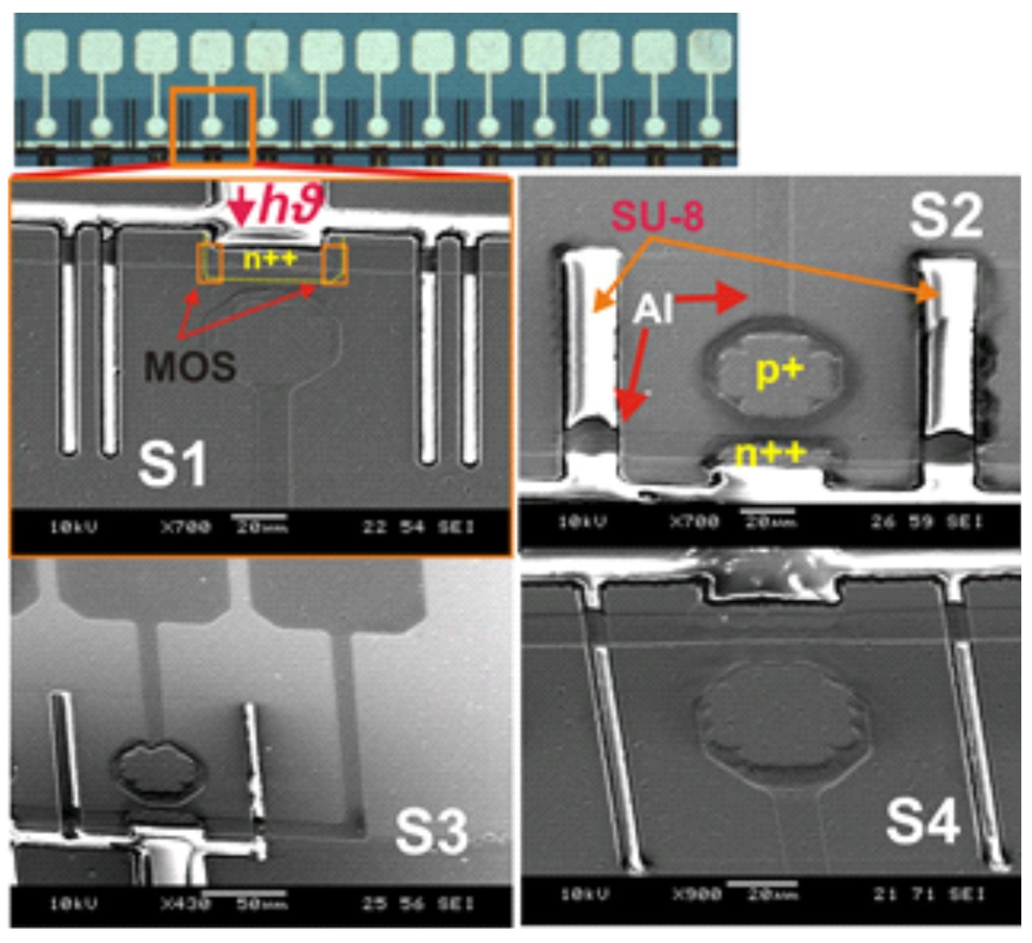
(a) Film stack. (b) Optical microscope image of the CISWDS device. One ...
TEM image of the cross section of a the n-channel FG FinFET transistor ...
(PDF) AlN Piezoelectric on Silicon MEMS Resonator with Boosted Q using ...
Schematic illustration and cross-sectional image of state-of-the-art ...
11: a) Integrated magnetic nanolayer for the actuation of a doubly ...
(Color online) Device schematic diagram, scanning electron micrographs ...
All-nitride C-shunt flux qubit consisting of epitaxially grown ...
Figure 1 from Hybrid InGaAs/SiGe CMOS circuits with 2D and 3D ...
Figure 2 from Improving the Cell Characteristics Using Low-k Gate ...
Micromachines | Free Full-Text | Self-Aligned Interdigitated ...
Fabrication process of typical EDLT devices based on layered materials ...
Cross section SEM micrograph of a Au/Sn solder joint after ...
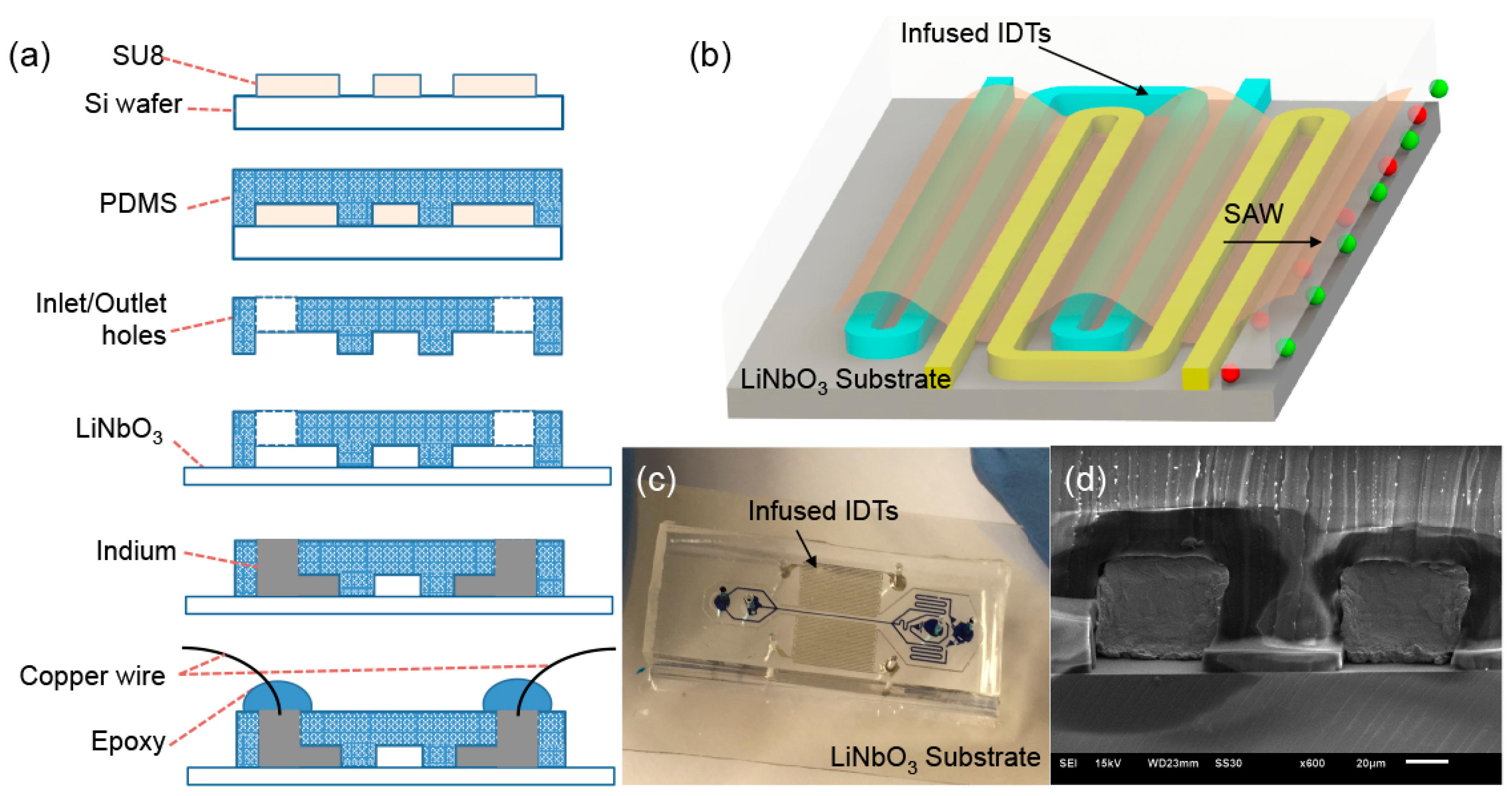
(a) Single MEMS pixel geometry (top view) (b) Fabrication steps: (1 ...
Design of the high-contrast grating (HCG) VCSEL. (a) Cross-sectional ...
(Top) Optical micrograph showing hydrophobic layer was processes (i.e ...
Figure 1 from Towards Enabling Two Metal Level Semi-Damascene ...
SEM images of the fabricated switches: a Plan view of a switch D1. The ...
Figure 1 from New methodology for modelling MOL TDDB coping with ...
Substrate patterned by thermal NIL. (a) Tilted scanning electron ...
(a) Top view of multiple fin array of InAs grown uniformly from Silicon ...
Optical microscope image of (a) the fabricated MDM resonance-enhanced ...
Photographs of the antenna test structures. Single element with probe ...
Silex microsystems:MEMS foundry services | MEMS Total Solutions ...
The optical micrograph image (a) and corresponding SEM image (b) of a ...
Optical microscopic images obtained for (a) Cu-Ni-Sn -bumps and (b) Au ...
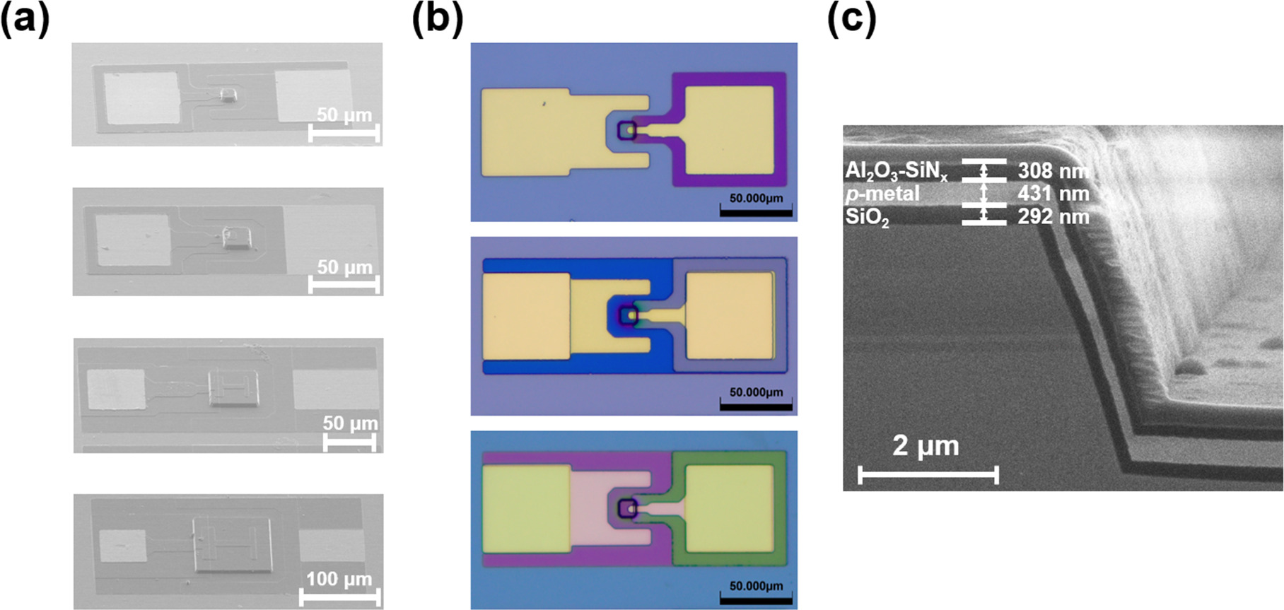
Photonics | Free Full-Text | Waveguide-Integrated Ge/Si Avalanche ...
The characterization of in situ TEM micro‐cantilever chip. a ...
SEM images of specimen fabricated by FIB. | Download Scientific Diagram
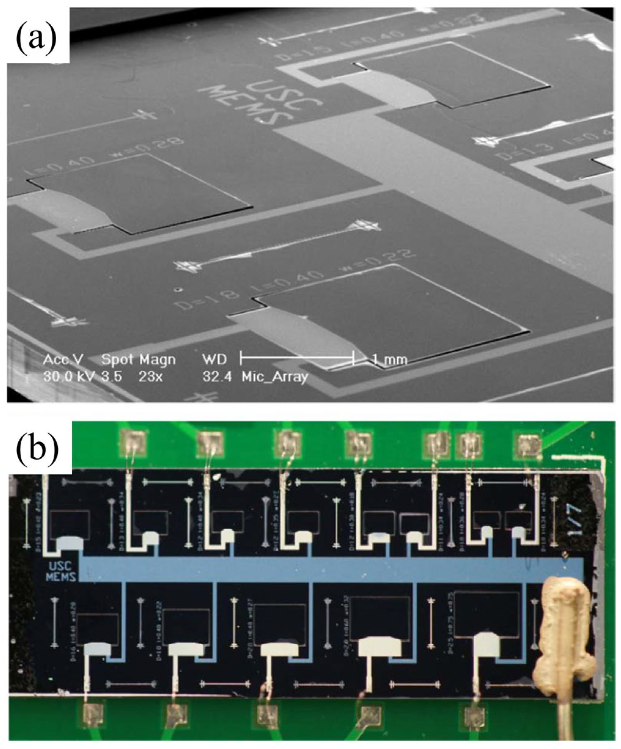
Micromachines | Free Full-Text | Micro-Electro-Mechanical Systems ...
Figure 16 from Wafer level system integration for SiP | Semantic Scholar
Figure 1 from Dimensionless Analysis of Micro Pirani Gauges for Broad ...
Improving the Electrical and Optical Characteristics of AlGaInP Red ...
a, b Physical structure of Si MOS QD. Five top gates marked ...
Epitaxial layer structure (a), microscope image and cross section of ...