Please enter url.
Login
Logout
Please enter url.
Cross section SEM micrograph of a Au/Sn solder joint after ...
researchgate.net
source
Comments
Proceedings | Free Full-Text | Analysis of pn Junction Deep Trench ...
POL(Power Overlay) | Services | SHINKO ELECTRIC INDUSTRIES CO.,LTD.
Electronics | Free Full-Text | Design and Implementation of RF Front ...
Pixelated diamond detector. | Download Scientific Diagram
Floating Metal (Cr/Au) pattern in: (a) SiO 2 based RF MEMS switch (b ...
SEM of RF MEMS capacitive switches after ESD shows the most probable ...
Novel design method optimizes performance of microelectromechanical ...
Modulation depth of series SQUIDs modified by Josephson junction area
Optical micrographs of fabricated AlN-on-Si Lamb wave resonators with ...
Plain optical images of (a) an actual S 0-LWR and (b) an SMR ...
Polysilicon side-wall friction test device fabricated at the Sandia ...
Novel Technology to Check Body Temperature with Smartphone Camera developed
Spectrometry? There's an app for that! • healthcare-in-europe.com
Figure 1 from A 0.0018-mm2 153% Locking-Range CML-Based Divider-by-2 ...
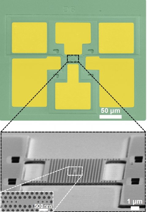
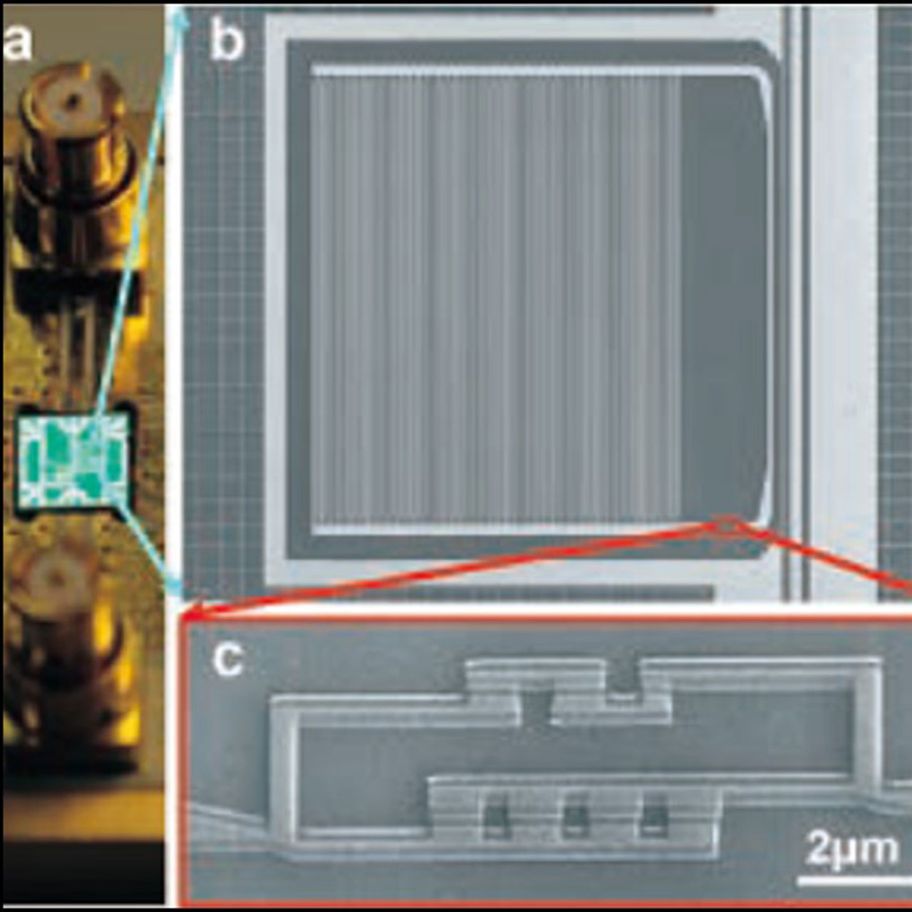
Photograph of test structure with single device with a total size of ...
Optical microscopic images obtained for (a) Cu-Ni-Sn -bumps and (b) Au ...
Design of the bump bond DC characterization hybrid. a) Photograph of a ...
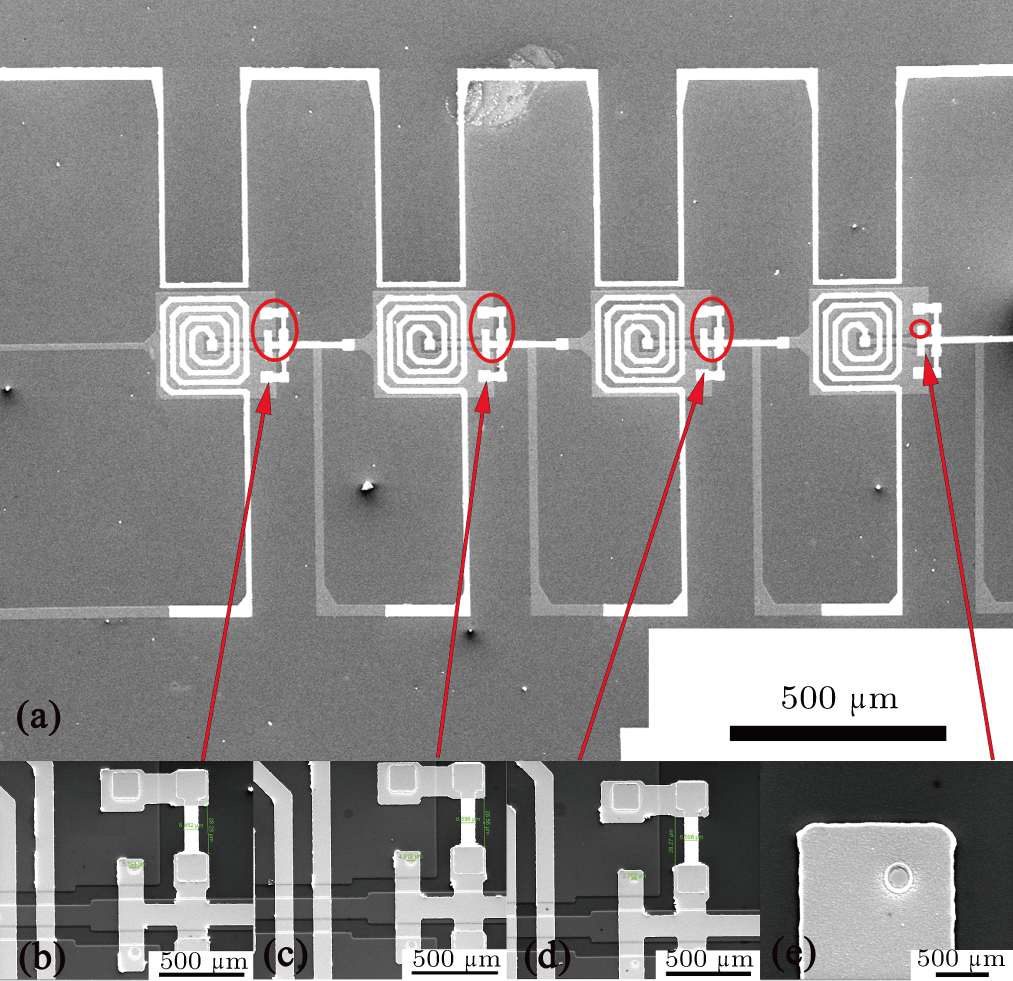
Part of the structure for the detection of defects in the M2 layer ...
Sensors | Free Full-Text | Design, Fabrication and Levitation ...
Advanced ICT Research Institute/NICT
Sensors | Special Issue : Ionic Liquids
Inspection: MVTec Software
Micromachines | Free Full-Text | Integrated Magnetic MEMS Relays ...
Photos of the fabricated inertial switch | Download Scientific Diagram
(a) Photograph of the fabricated MEMS energy harvesting chip; the inset ...
Configurations and dimensions of TAV substrate with Cu via and films ...
Single-cell trapping-based approaches: single cell trapping array: (A ...
a Electrostatic scanner's photo, b CCD camera images of the ...
Figure 1 from Tungsten grid enhanced thin-film wafer-level ...
Figure 3 from Design and fabrication considerations in developing high ...
BioMEMS Research Group
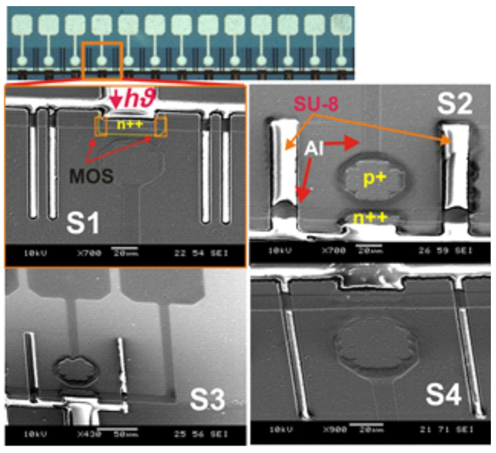
Wafer with U3DTHIN detectors set of mask and SEM images | Download ...
Stacking microLEDs onto a full-CMOS active matrix, with micro t...
| (A) Schematic cross-section of a pixel detector module assembly: (1 ...
Micromachines | Free Full-Text | A Non-Sacrificial 3D Printing Process ...