Please enter url.
Login
Logout
Please enter url.
Fabrication process of typical EDLT devices based on layered materials ...
researchgate.net
source
Comments
Fabrication process of typical EDLT devices based on layered materials ...
Schematic illustration and cross-sectional image of state-of-the-art ...
Conceptual illustration of the microfluidic check valve based on ...
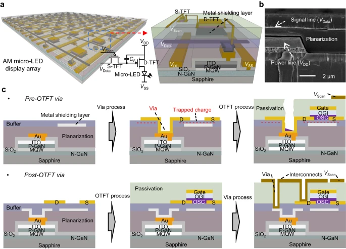
Researchers develop new method for OTFT integration in microLED planes ...
Schematic diagram of pattern preparation, Mo film deposition and ...
(a) Schematic diagram of the piezoresistive cantilever. (b) Photographs ...
(a) Film stack. (b) Optical microscope image of the CISWDS device. One ...
The iterative imprint and etch process. a) The schematic of a primary ...
Exemplar chip-scale integration schemes. (a) An InP laser integrated ...
Schematic process flow. Nanogaps are created by shadow evaporation of ...
The schematic image and the pictures of the epoxy drops on the ...
(a) Process for transfer of polyimide films by rolling [195] and (b ...
Figure 1 from NexFET generation 2, new way to power | Semantic Scholar
(a) Schematic of the EFISH device layout. (b) Secondary electron ...
Schematics and cross sections of the hybrid III-V/Si SOAs designed by ...
Plain optical images of (a) an actual S 0-LWR and (b) an SMR ...
Schematic illustration of (a) hybrid and (b) heterogeneous integration ...
(a) Optical microscopy image of a microwire device after the lift-off ...
(a) Schematics of the double-tape-assisted Micro-LED transfer printing ...
Proceedings | Free Full-Text | Analysis of pn Junction Deep Trench ...
(a) Fabrication process for the S1 Lamb mode resonator. (b) SEM of the ...
SUNY Poly Researchers Advance Bipolar Junction Transistors in Two ...
Figure 1 from Dimensionless Analysis of Micro Pirani Gauges for Broad ...
Bolometer device [IMAGE] | EurekAlert! Science News Releases
Micromachines | Free Full-Text | Self-Aligned Interdigitated ...
Figure 1 from Plasmonic-Assisted Mach-Zehnder Interferometric Photonic ...
(PDF) 80 GHz germanium waveguide photodiode enabled by parasitic ...
Figure 1 from Destructive Little-Parks Effect in a Full-Shell Nanowire ...
Improving the Electrical and Optical Characteristics of AlGaInP Red ...
4: Prototype of the fabricated MEMS probe card. (a) Scanning electron ...
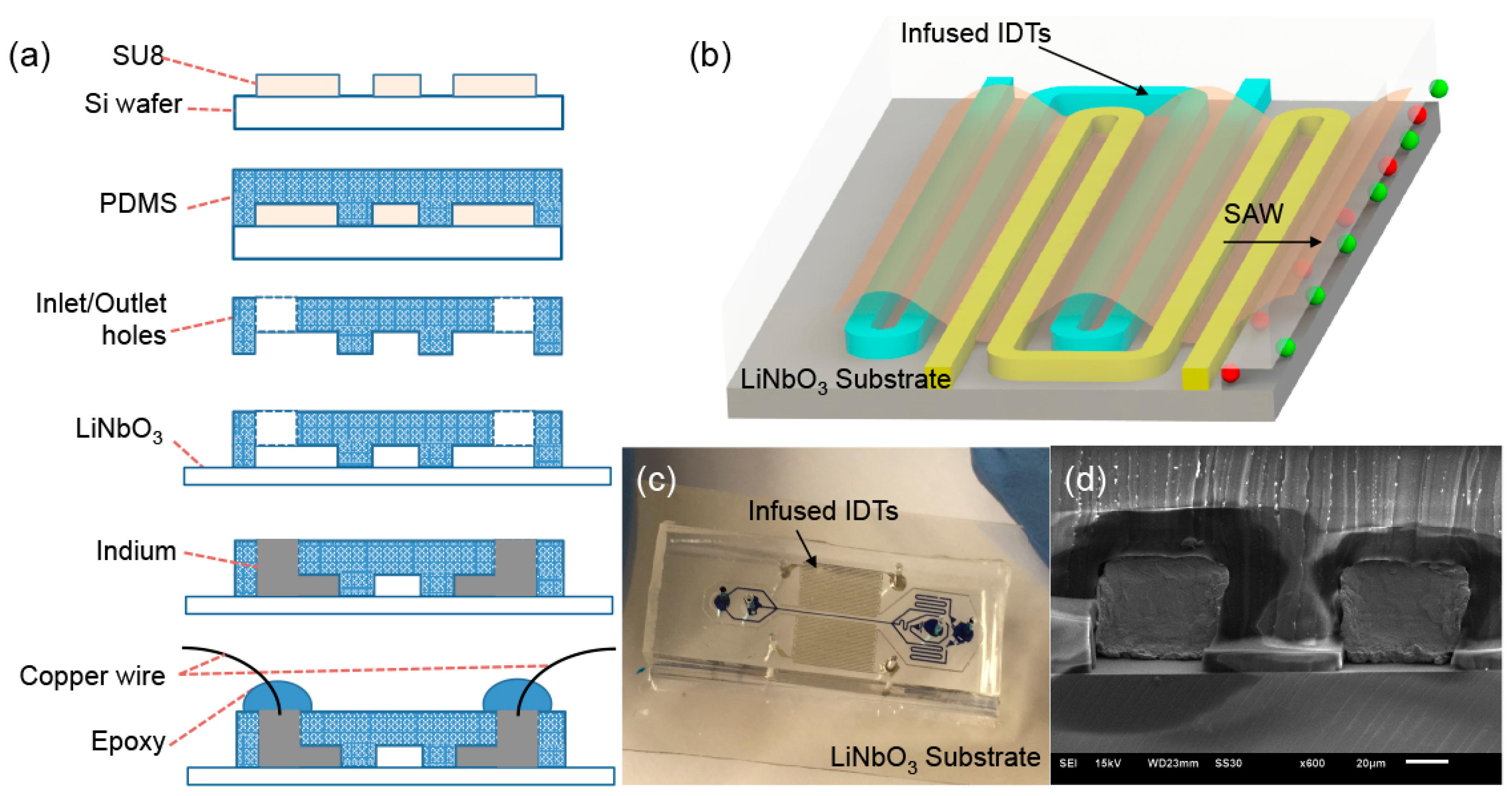
Design and image of the self-aligned SAW-based microfluidic device. (a ...
Illustration of (a) schematic diagram of the fabricated glucose sensor ...
(a) Schematic of the metal nanosheet sensor array. Crosssectional TEM ...
( a ) The fabricated Si platform, the magnified views of the Si ...
Inkjet Printing of High Performance Transistors with Micron Order ...