Please enter url.
Login
Logout
Please enter url.
(Top) Optical micrograph showing hydrophobic layer was processes (i.e ...
researchgate.net
source
Comments
(Top) Optical micrograph showing hydrophobic layer was processes (i.e ...
(A-G) Fabrication process for the dielectric film with a single ...
Possible computer data storage system smaller than a dot on this page ...
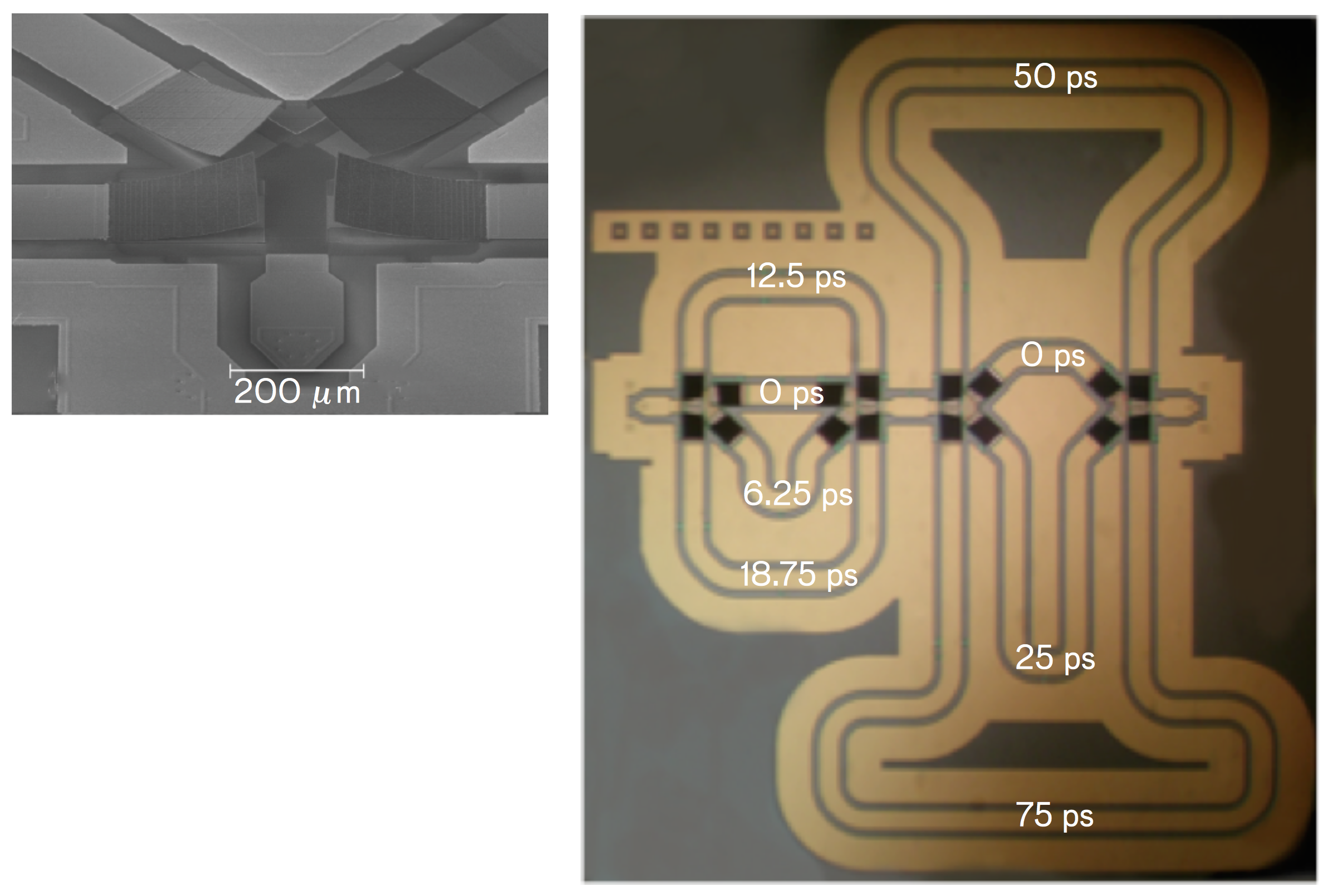
Schematic view and SEM image of SINIS bolometer with a normal metal ...
Figure 1 from Coulomb blockade and coherent single-cooper-pair ...
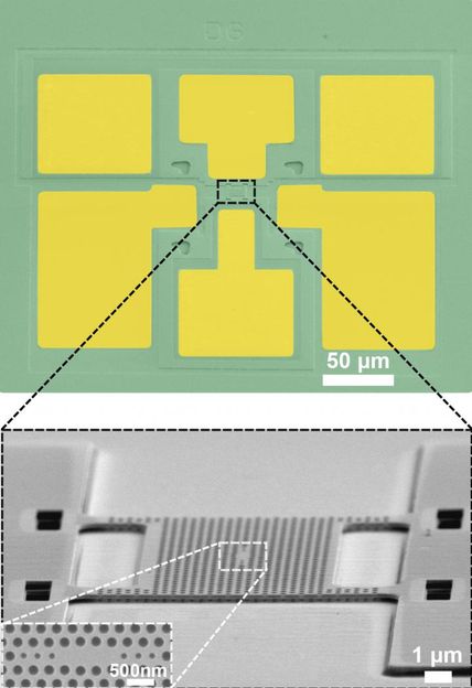
SEM image of PD (a) with sacrificial layer; (b) supported by SiN x ...
Tech Notes
Fabricated structure. (a) Scanning electron micrograph, top view. (b ...
Micro-spectrometer opens door to a wealth of new smartphone functions
An optical micrograph of a fully integrated and passivated microband ...
Sensitivity enhancement for micromechanical vibro‐impact resonators ...
(a) SEM images of polymer-filled MWCNT arrays, and (b) optical images ...
Scanning electron microscope (SEM) images. a A general view of the RF ...
Biomimetic Flow Sensors | SpringerLink
Science Codex | Science news, science articles, all day, every day
Research Outreach: Using Insects To Develop Microphones & Transducers
Nanomaterials | Free Full-Text | Tailoring InSb Nanowires for High ...
(PDF) Proximity effect in PbTe-Pb hybrid nanowire Josephson junctions
Fabricated accelerometer. (a) Chip photo and (b) close-up SEM image ...
The Tiniest 1nm Gate Transistor - Electronics-Lab.com
Smallest nanobridge obtained by etching at elevated (-80C) temperature ...
Microphotographs and images representing the different steps of the ...
The rectangle in the center is a thin LT-GaAs layer on the HR-Si ...
9: SEM image of a 3-dimensional nanoSQUID fabricated using FIB ...
Combined UV & e-beam lithography patterning in a mix & match approach ...
Plain optical images of (a) an actual S 0-LWR and (b) an SMR ...
Vertically Aligned Carbon Nanotubes as Platform for Biomimetically ...
Cross-sectional view of integrated micromirror array, showing the ...
Spintronics Driven by Superconducting Proximity Effect | IntechOpen
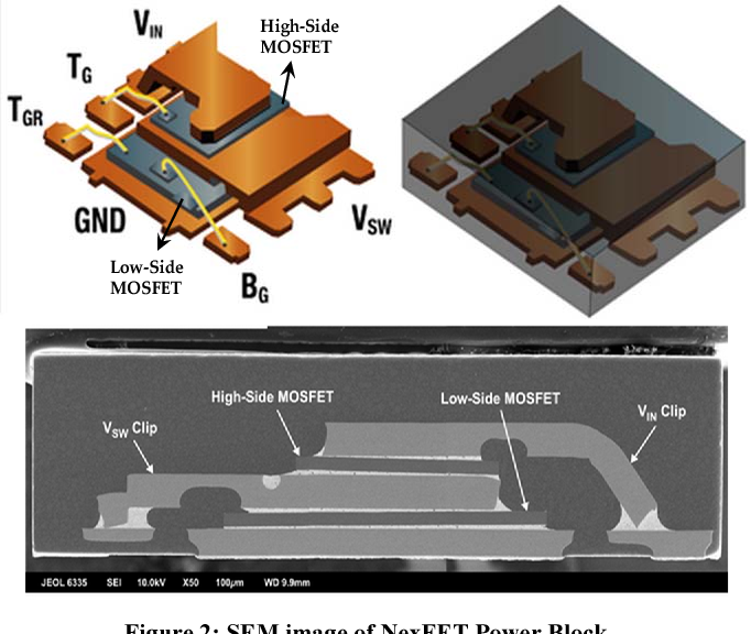
Figure 2 from NexFET generation 2, new way to power | Semantic Scholar
A rapid and simple method to draw polyethylene nanofibers with enhanced ...
(Color online) Device schematic diagram, scanning electron micrographs ...
FET with HfO 2 (20 nm)/Parylene-C (6 nm) solid-state bilayer gate ...
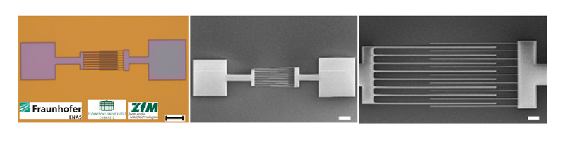
Suspended high Q integrated inductor by wafer level packaging ...
Observation of fluctuation-mediated picosecond nucleation of a ...