


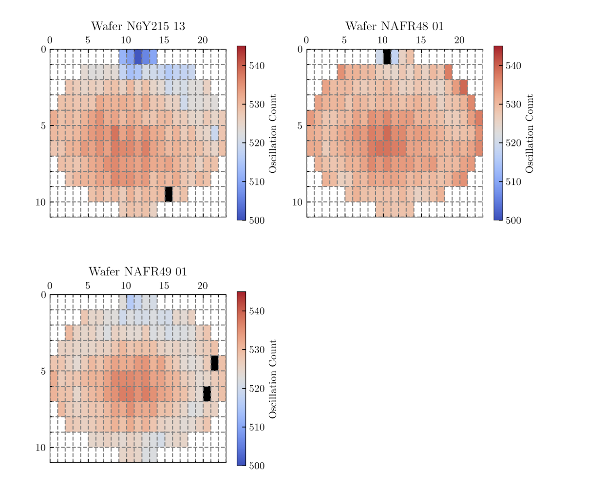

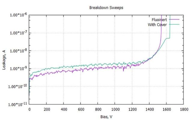


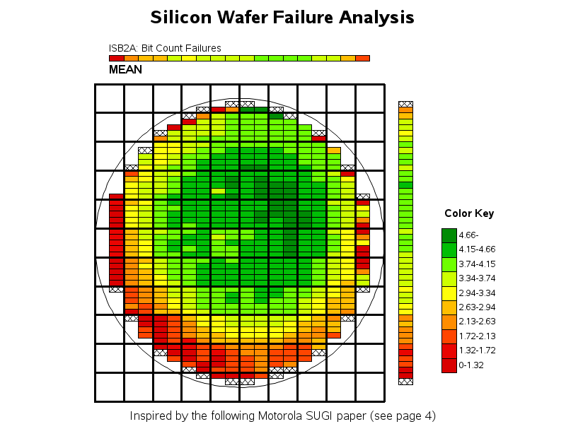

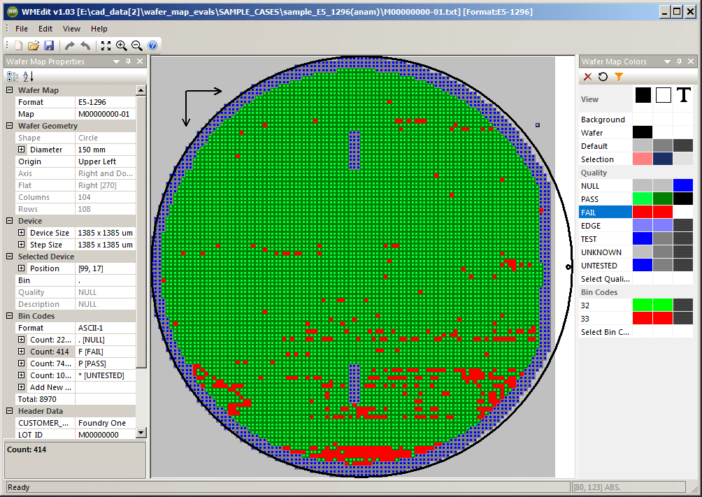
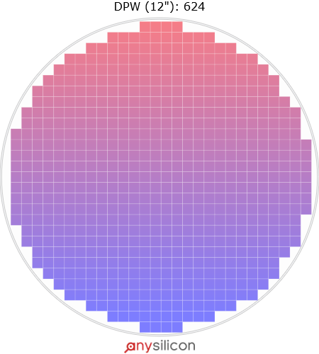


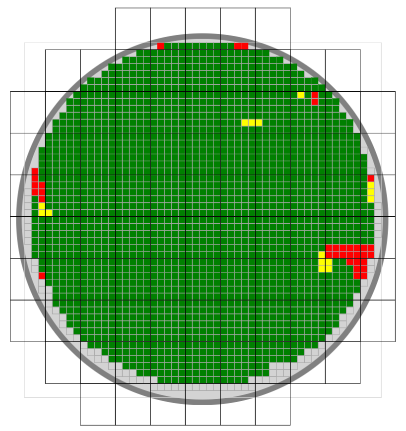


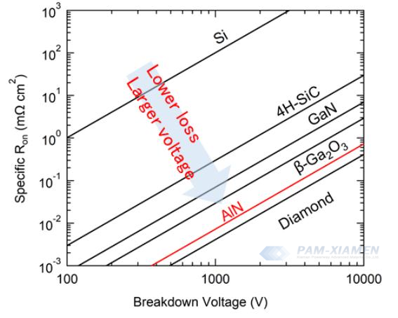


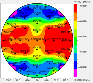


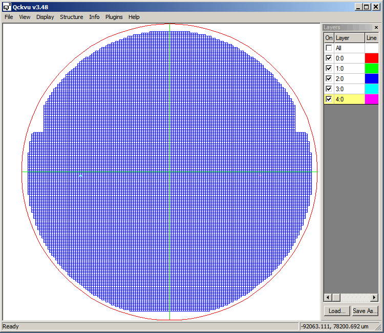


Utilize our extensive wafer maps of the breakdown voltages for test wafers which exhibited resource library containing vast arrays of high-quality images. captured using advanced photographic techniques and professional equipment. meeting the demanding requirements of professional projects. Discover high-resolution wafer maps of the breakdown voltages for test wafers which exhibited images optimized for various applications. Perfect for marketing materials, corporate presentations, advertising campaigns, and professional publications All wafer maps of the breakdown voltages for test wafers which exhibited images are available in high resolution with professional-grade quality, optimized for both digital and print applications, and include comprehensive metadata for easy organization and usage. Each wafer maps of the breakdown voltages for test wafers which exhibited image meets rigorous quality standards for commercial applications. Advanced search capabilities make finding the perfect wafer maps of the breakdown voltages for test wafers which exhibited image effortless and efficient. Each image in our wafer maps of the breakdown voltages for test wafers which exhibited gallery undergoes rigorous quality assessment before inclusion. Diverse style options within the wafer maps of the breakdown voltages for test wafers which exhibited collection suit various aesthetic preferences. Comprehensive tagging systems facilitate quick discovery of relevant wafer maps of the breakdown voltages for test wafers which exhibited content.