Please enter url.
Login
Logout
Please enter url.
Loading ...
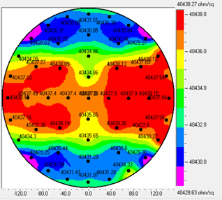
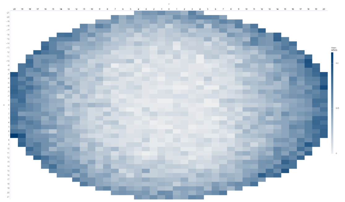
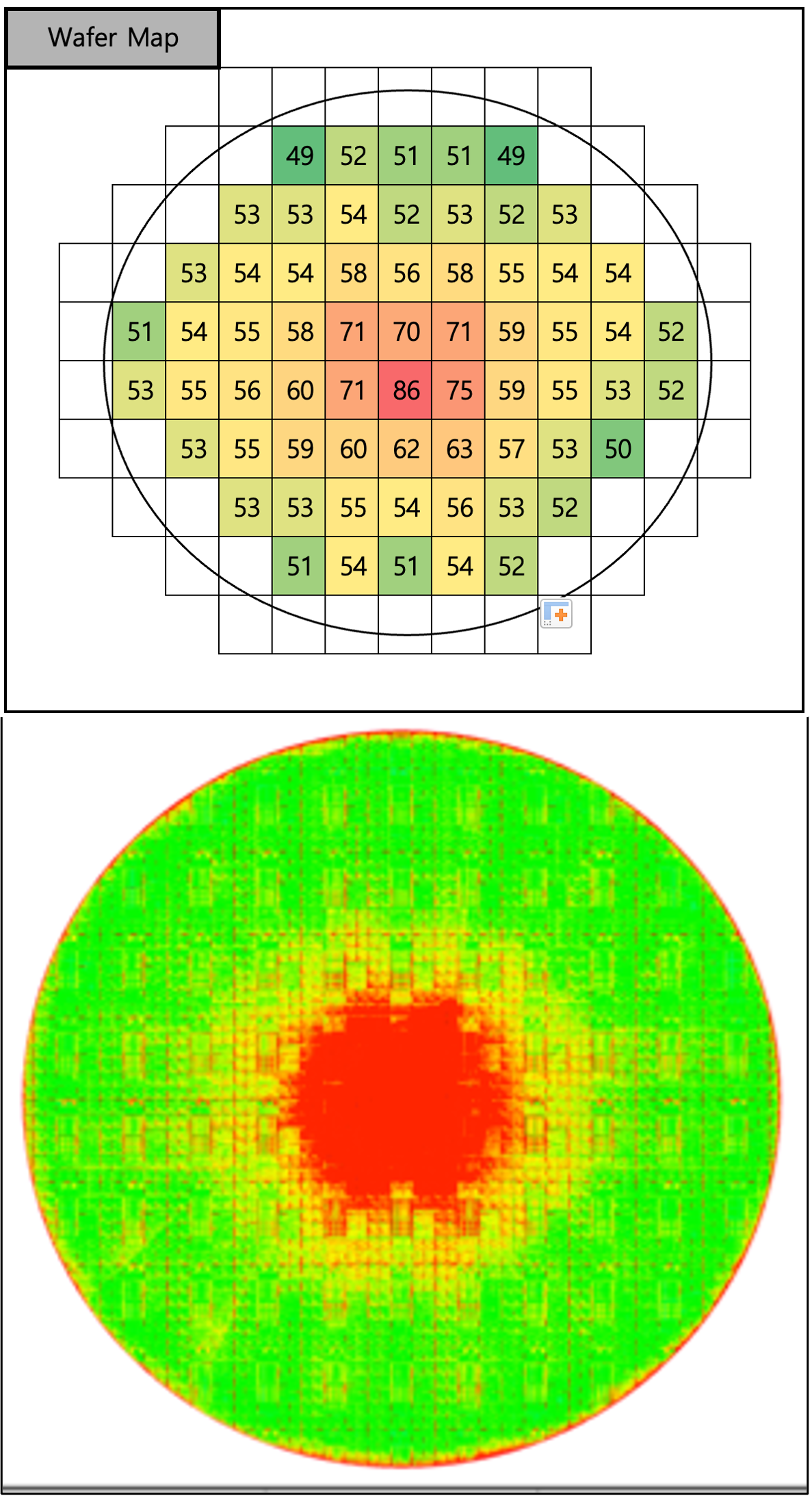
Wafer Defect Map
Wafer_Map_Defect_Pattern_Classification/Wafer_Map_Defect_Classification ...
Techniques to Identify and Correct Asymmetric Wafer Map Defects Caused ...
Methods to Establish and Right Uneven Wafer Map Defects Attributable to ...
Wafer Map Failure Pattern Classification Using Geometric , 53% OFF
Techniques to Identify and Correct Asymmetric Wafer Map Defects Caused ...
Wafers-Defect-Recognition-using-Visual-Transformer/MixedDefectWafer_ViT ...
Figure 3 from Clustering Wafer Defect Patterns Within the Semiconductor ...
Wafer Bin Map Defect Classification Using Semi-Supervised Learning
Figure 1 from Clustering Wafer Defect Patterns Within the Semiconductor ...
Figure 2 from Clustering Wafer Defect Patterns Within the Semiconductor ...
Techniques to Identify and Correct Asymmetric Wafer Map Defects Caused ...
Figure 1 from Clustering Wafer Defect Patterns Within the Semiconductor ...
Figure 1 from Clustering Wafer Defect Patterns Within the Semiconductor ...
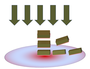
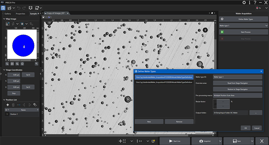
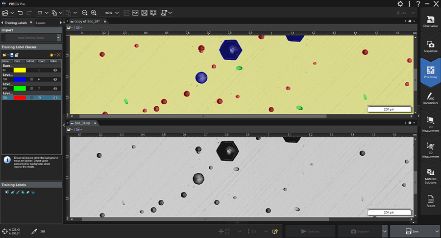
Defect Detection on Etched Silicon Carbide (SiC) Wafers
Generate defect data of a wafer map
Generate defect data of a wafer map
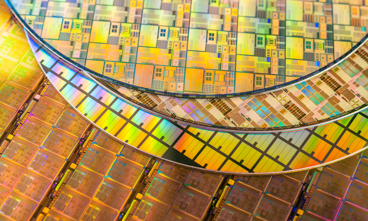
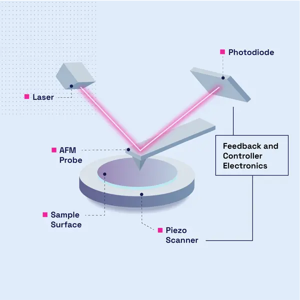
Semiconductor Wafer Microscope
Defect Detection on Etched Silicon Carbide (SiC) Wafers
利用晶圆图提高集成电路良率 | Enhance Integrated Circuit Yields with a Wafer Map
Wafer Analysis Service – IMSEMICON
Wafer Analysis Service – IMSEMICON
Wafer Analysis Service – IMSEMICON
Wafer Analysis Service – IMSEMICON
Top 5 Wafer Inspection Tools for Semiconductor… | Robovision
Explore Silicon Carbide, Crystal Growth, and Wafer Processing
What Is Wafer Annealing and What Role Does It Play in the Semiconductor ...
Explore Silicon Carbide, Crystal Growth, and Wafer Processing
Top 5 Wafer Inspection Tools for Semiconductor… | Robovision
昇美達國際開發股份有限公司ge-wafer
Top 5 Wafer Inspection Tools for Semiconductor… | Robovision
Visual inspection equipment for wafers (before dicing)|Products|HU ...
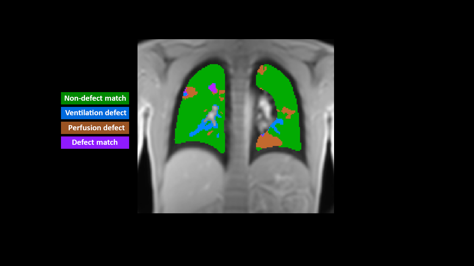
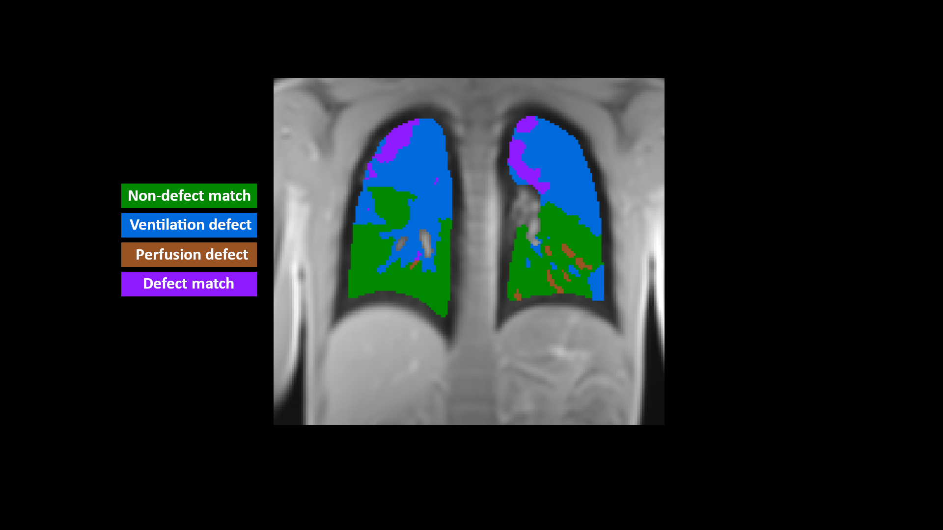
LungMaps - Siemens Healthineers India
What Is Wafer Annealing? | Wafer World
LungMaps - Siemens Healthineers India
Semi Cera: Silicon on Insulator Wafer: Hidden Drawbacks
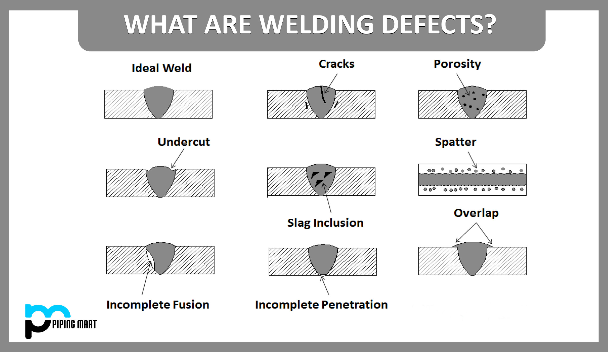
What Is Undercut In Welding Diagram Chart 1 0 Modern Design - Ponasa
昇美達國際開發股份有限公司ge-wafer
Explore PEMTRON’s Advanced Imaging for Defect Detection at SEMICON ...
Unlocking the Power of Float Zone Silicon Wafers: Terahertz ...
Semi Cera: How Silicon Carbide Dummy Wafers Revolutionize Semiconductor ...
Toshiba Develops of Optical Inspection Technology for One-Shot 3D ...
Country Life Folate 400 mcg 100 Chewable Orange Wafer | Nahdi Online ...
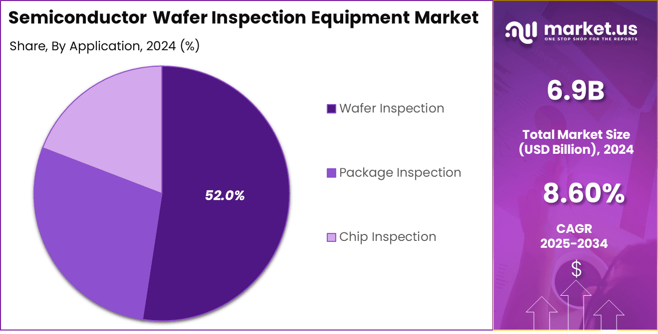
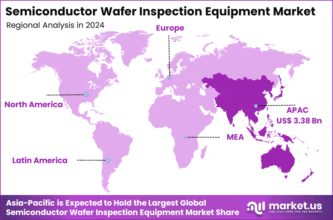
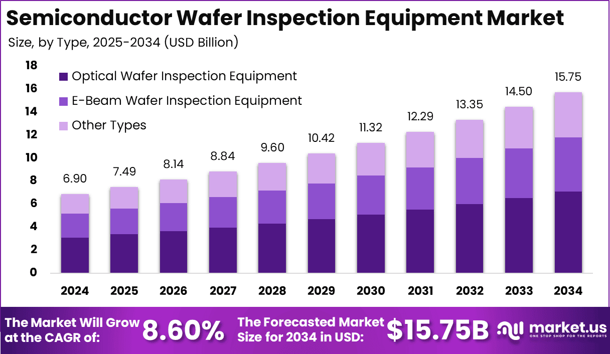
Semiconductor Wafer Inspection Equipment Market | CAGR 8.60%
Top 5 Wafer Inspection Tools for Semiconductor… | Robovision
Unlocking the Power of Float Zone Silicon Wafers: Terahertz ...
Case study - Wafer clamp ring| Ensinger
Wafer Laser Cutting Machine Manufacturers, Suppliers - Good Price - HGLASER
JMP软件中的晶圆图( Wafer Map)分析_word文档在线阅读与下载_免费文档
Semiconductor Wafer Inspection Equipment Market | CAGR 8.60%
Used Tc Wafer Kla for sale. KLA-Tencor equipment & more | Machinio
3C-SiC Homoepitaxial Wafer for Reliable MOSFETs
Used Tc Wafer Kla for sale. KLA-Tencor equipment & more | Machinio
TSV Defect Inspection-Applications-Spirox Corporation
JMP软件中的晶圆图( Wafer Map)分析_word文档在线阅读与下载_免费文档
Semiconductor Wafer Inspection Equipment Market | CAGR 8.60%
Sigma W8: Automated Wafer Testing Made Simple | xyztec bv
Explore Silicon Carbide, Crystal Growth, and Wafer Processing
Sigma W8: Automated Wafer Testing Made Simple | xyztec bv
C# wafer map, 晶圆膜厚,rs, 色温图-CSDN博客
Wafer Paper and Tile Cake - Guest Instructor Laura Saporiti - April 1st ...
A defect in the enzyme that catalyzes the formation | Chegg.com
Steel surface defect detection based on bidirectional cross-scale ...
Used Gem Handler for sale. KLA-Tencor equipment & more | Machinio
A steel surface defect detection method based on improved RetinaNet ...
FWF30016-D18S23K6M Wafer 3mm, 18Circuits, Vertical(180°), SMT
Video: Procedure for the Transfer of Polymer Films Onto Porous ...
Semiconductor Wafer Defects
Wafer Defect Image
Wafer Bin Map
Wafer Mapping
Wafer Shot Map
Defect Heat Map
Wafer Particle Map
Wafer Map Analysis
Wafer Map Patterns
Wafer Die Map
Wafer Map Block
Wafer Map Similarity
Types of Wafer Defects
Spotfire Wafer Map
Klarity Wafer Map
Gel Defect Wafer
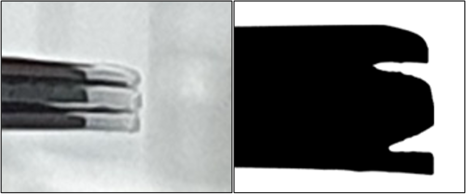
Picture of Wafer Sidewall Defects
Wafer Edge Map
Wafer Defect Fail Map
Echart Wafer Map
Wafer Map Xy
Cumulative Defect Map
Wafer Line Map
Wafer Map Doughnut
Lam Wafer Map
Stdf Wafer Map
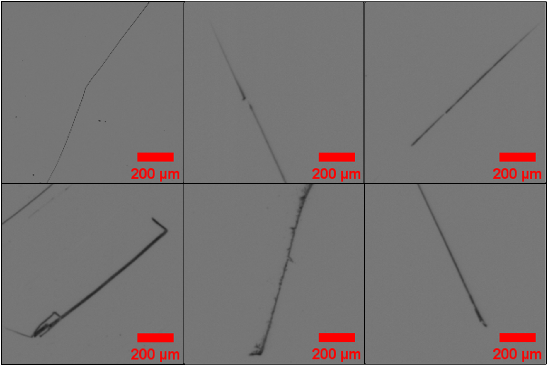
Example of Defect On Wafer
Wafer Map Zone
Wafer Map Donut
Wafer Map Clustering
Thickness Wafer Map
Ecid Wafer Map
Wafer Map Fails
Shifted Wafer Map
Wafer Map Dpat
Dislocation Wafer Map
Silicon Wafer Map
Stif Wafer Map
Wee Map Wafer
Curve Defect Map
Wafer Map Stack
SIC Wafer Defect Map
JMP Wafer Map
Chip Wafer Map
Wafer Map Correlation
EWS Wafer Map
Nexperia Wafer Map
Contoure Map Wafer
Wafer Map Defect by Chamber
MATLAB Wafer Map