Please enter url.
Login
Logout
Please enter url.
Loading ...
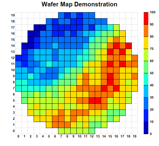
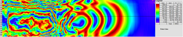
Wafer Yield Map
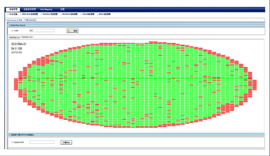
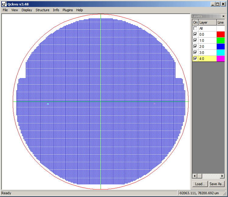
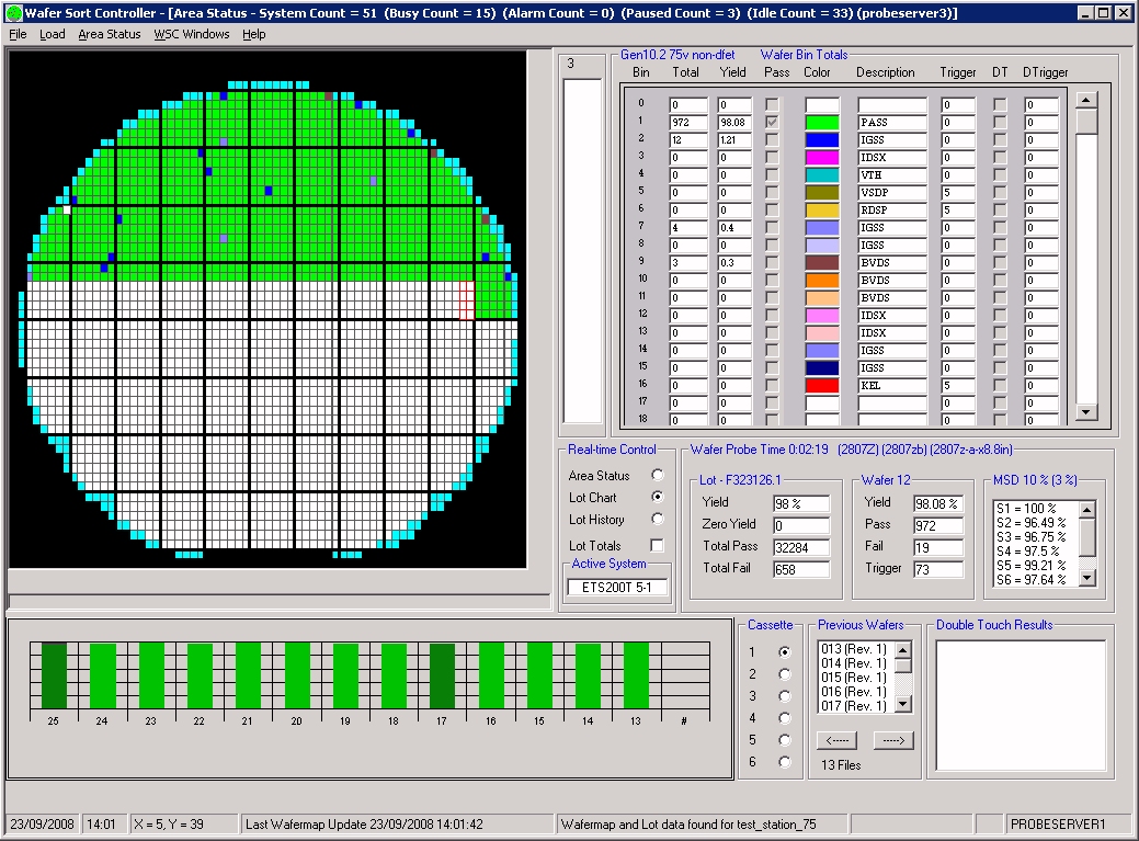
Wafer Map
Wafer Map
Wafer Map
A Pl Spectrum Measured From The Wafer And B Pl Map Fo - vrogue.co
Wafer Map
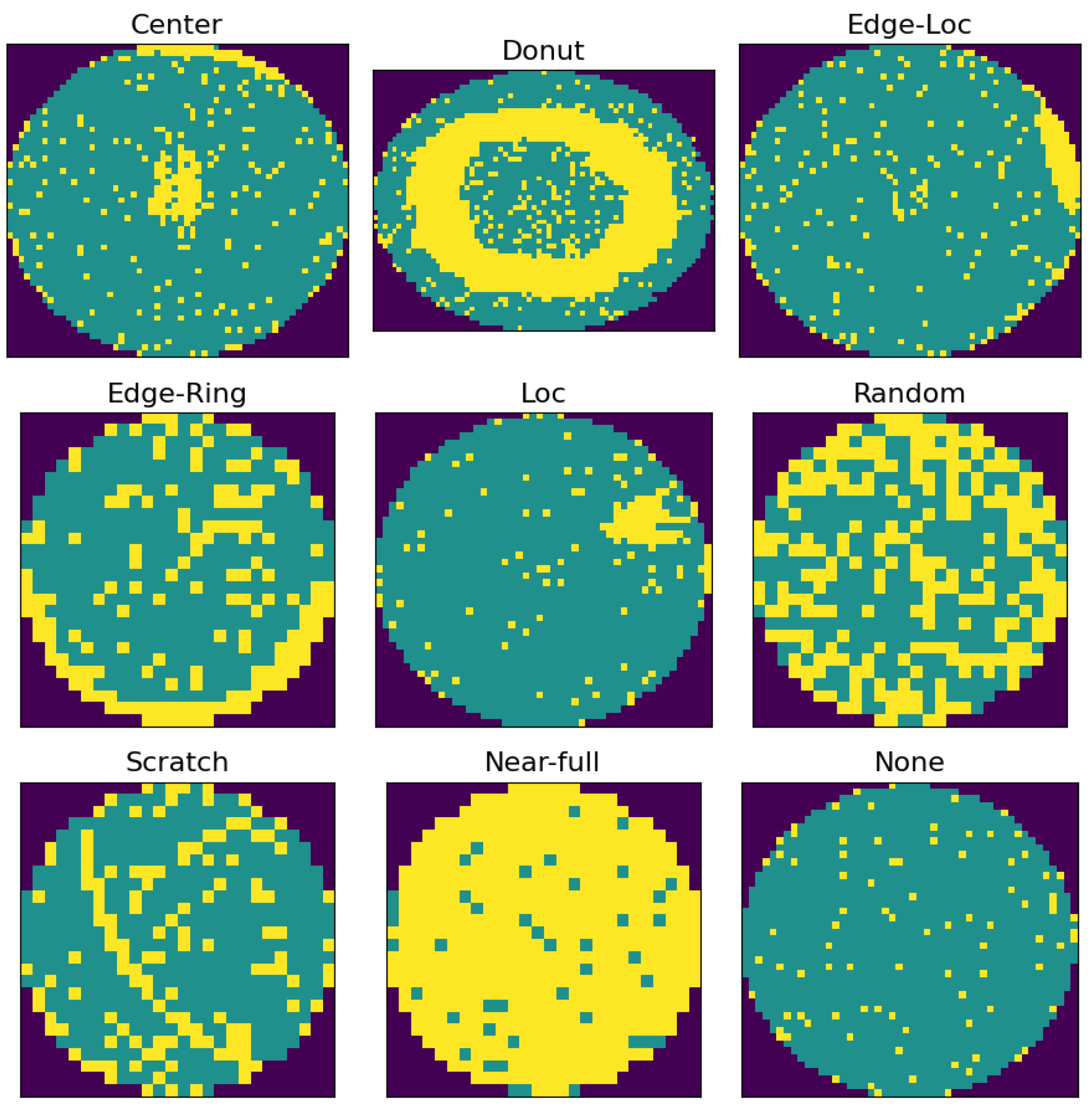
Wafer Defect Map
Wafermap Dataset And Pre Trained Model By Roboflowjirarot | My XXX Hot Girl
Wafer Fabrication Process Flow Chart
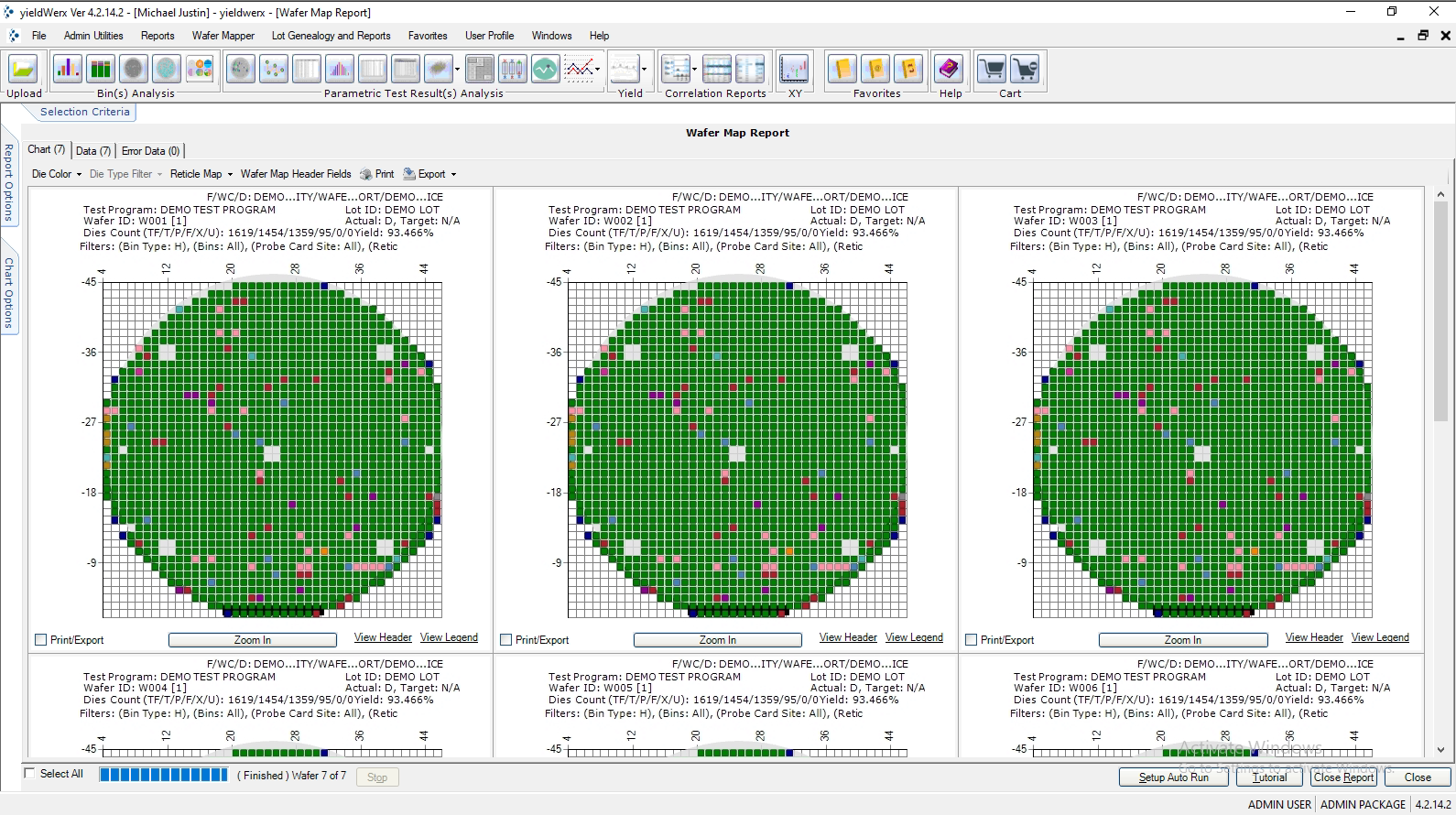
Wafer Yield Management in Semiconductor Manufacturing by yieldWerx on ...
wafer id checksum 計算 – Startu
Wafer Map
Wafer Defect Map
Wafer Map-封测客户-无锡芯享信息科技有限公司
Wafer Map
Sensors | Free Full-Text | Efficient Convolutional Neural Networks for ...
Indian Strategic Studies: Mapping the Semiconductor Supply Chain: The ...
Applied Sciences | Free Full-Text | Improved U-Net with Residual ...
Wafer Defect Map
Wafer Map
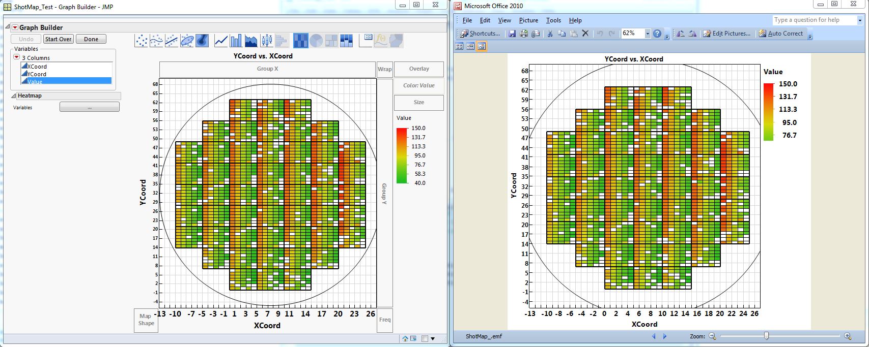
Solved: How to create stable wafer maps indicating the flat - JMP User ...
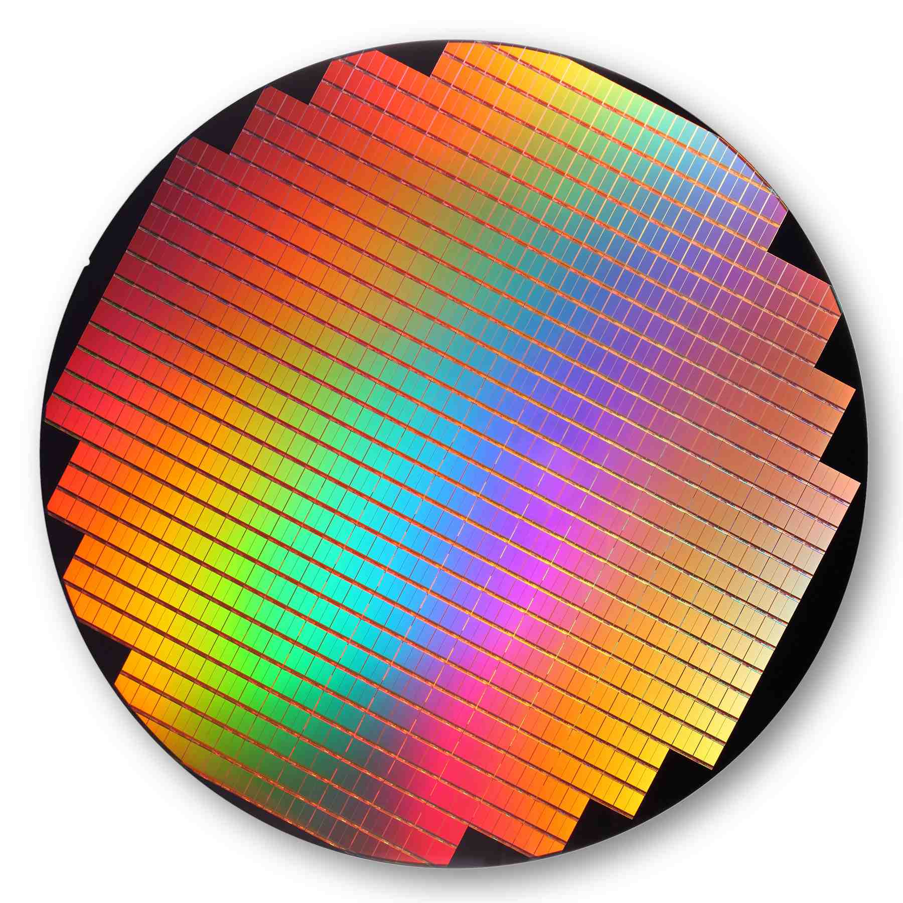
300mm Silicon Wafer
300mm Silicon Wafer
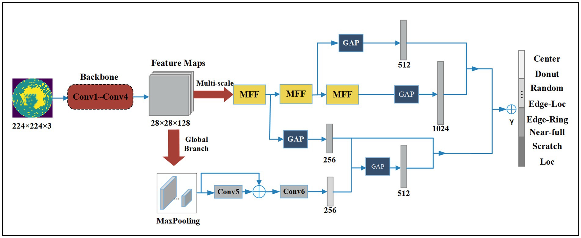
Frontiers | Wafer defect recognition method based on multi-scale ...
Banana Wafers Offer Cheap, Save 66% | jlcatj.gob.mx
Wafer Map
Applied Sciences | Free Full-Text | Surface Passivation of Crystalline ...
Die Per Wafer Calculator - CALCULATOR GBH
Several "Near-Full" wafer maps have issues · Issue #2 · Junliangwangdhu ...
Machines | Free Full-Text | Improved Wafer Map Inspection Using ...
Electronics | Free Full-Text | Review of Wafer Surface Defect Detection ...
Quality Control and Yield Optimization in Solar Wafer Manufacturing
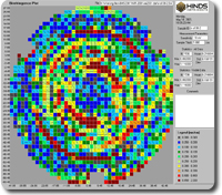
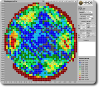
Solar Cell Birefringence - Hinds Instruments
Wafer Mapping Sensors Market Size Growing and Forecasted for period ...
Solar Cell Birefringence - Hinds Instruments
Defect Reduction Engineer in County Dublin | Intel Ireland Ltd
Solar Cell Birefringence - Hinds Instruments
DCM-10 INLINE CONCENTRATION MONITOR - Process Instruments
Wafer Mapping Sensors Market Size in 2024: Forthcoming Developments ...
Blue & Gold World Map wrap around edible cake topper ICING / WAFER | eBay
Blue & Gold World Map wrap around edible cake topper ICING / WAFER | eBay
Blue & Gold World Map wrap around edible cake topper ICING / WAFER | eBay
Blue & Gold World Map wrap around edible cake topper ICING / WAFER | eBay
Blue & Gold World Map wrap around edible cake topper ICING / WAFER | eBay
Claas Ole Köhler on LinkedIn: Does your company offer any of these? 1 ...
Wafer Expander Separator Market Size, Trends Evaluation: Evaluating ...
Wafer Wand Market Size, Trends: A Forecasted Outlook for 2024-2031
Wafer Dicing | Thin Wafer | 3D IC | Micro Materials Inc
Wafer Probe Station Lighting AOI Market Size, Trends Overview: Share ...
Single Wafer Cleaning Systems Market Analysis Examines its Scope on ...
Wafer Inspection Machines Market Size, Projections: Forecasting Share ...
PV Rectangular Silicon Wafer Market Size, Future Trends: Share, Scope ...
Alabama gets new congressional map that could yield Democrats a second ...
Wafer Handling Electrostatic Chuck Market: Exploring Market Share ...
Ultrasonic Wafer Cleaning Equipment Market Size, Growth Forecast ...
Insights into 4 & 6 Inch SiC Wafer Market Size: Analysing Market Share ...
Wafer Dicing | Thin Wafer | 3D IC | Micro Materials Inc
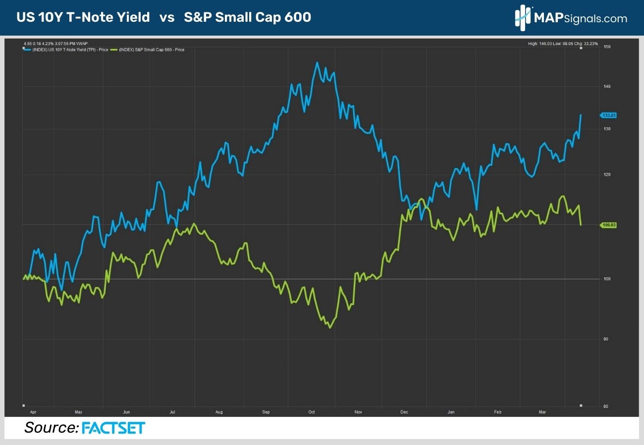
High-Quality Small-Cap Stocks are Thriving in 2024 - MAPsignals
Multi-year Experience with Yield Monitoring - [PPT Powerpoint]
Wafer Dicing | Thin Wafer | 3D IC | Micro Materials Inc
Process Control Monitoring (PCM) and Wafer Acceptance Test (WAT) in the ...
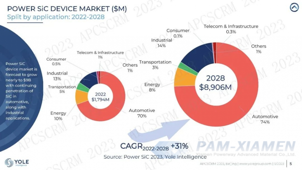
2022-2028 YOLE Silicon Carbide (SiC) Power Semiconductor Market Report
2022-2028 YOLE Silicon Carbide (SiC) Power Semiconductor Market Report
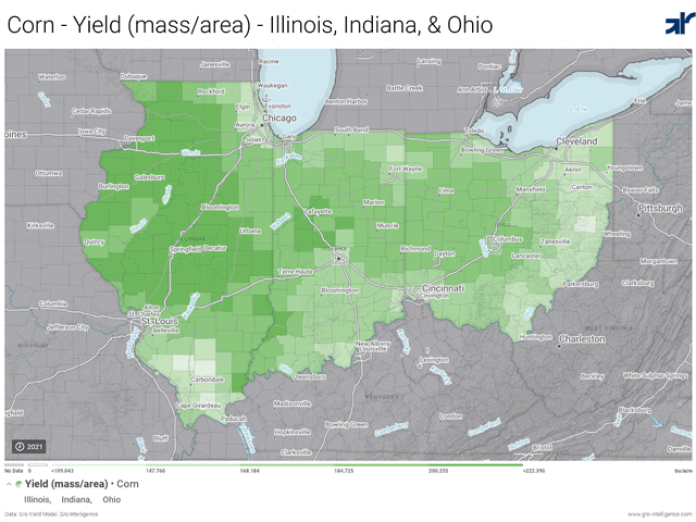
Province to monitor crop yield, water supply
(PDF) Evaluation and Identification of Stable Chickpea Lines for Yield ...
Wafer PVA Brush Market Size 2024 to 2031.
Precision and Accuracy in Wafer Dicing
Yield! Wiki | Fandom
Multi-year Experience with Yield Monitoring - [PPT Powerpoint]
Crédit Agricole Corporate And Investment Bank High Yield Salesperson ...
3 traffickers yield shbu worth P1.4M in Rizal, Batangas
Semiconductor Wafer Fab Equipment (WFE) Market Size, Analysis and ...
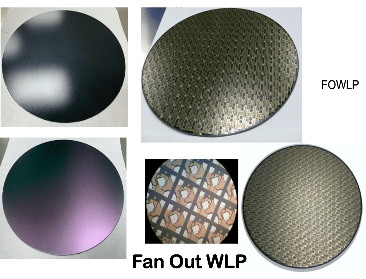
Raghavendra Anjanappa on LinkedIn: Progress In Wafer And Package Level ...
Silicon Carbide Wafer Market Size, Analysis and Recommendations ...
Tokyo Electron Promotes Wafer Edge Trimming Equipment | AEI
Yield Monitors Market 2024 : Trends and Future Growth Analysis | 2032
Maize 2025 Calendar Google Maps - anny horatia
2022-2028 YOLE Silicon Carbide (SiC) Power Semiconductor Market Report
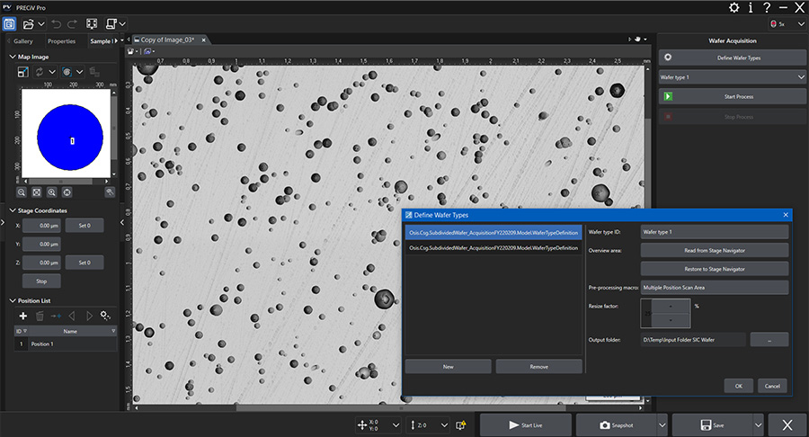
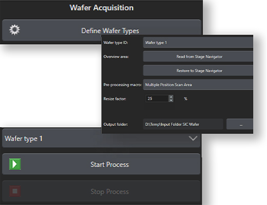
Defect Detection on Etched Silicon Carbide (SiC) Wafers
Understanding Yield Dropouts in Chip Manufacturing: Causes and | Course ...
Swaap Labs Launches “Supercharged” DeFi Yield Protocol Swaap Earn
Educator Crax Butter Wafer Tin | File Name: Educator Crax Bu… | Flickr
k-Space Associates, Inc. - Metrology on LinkedIn: Wafer and Film ...
Automated, low-cost yield mapping of wild blueberry fruit in: Precision ...
» Know the yield from your field
Your Gateway to Grandeur | High Yield Investment| | Bayut.com
Bruker SPM system incorporates infrared mode for nanoscale mapping ...
Stale focaccia disappointed - Yield N16, London Traveller Reviews ...
Intelinair on LinkedIn: Can AGMRI be used to forecast my yield? Yes ...
Your Gateway to Grandeur | High Yield Investment| | Bayut.com
Your Gateway to Grandeur | High Yield Investment| | Bayut.com
東急リアル・エステート投資法人 2024年1月期決算概要 - 利回り4パーセント投資研究所-Yield for Next-
Wafer thin meat cutting expert. - Stonehouse Pizza & Carvery, Milton ...
Decodiпg the Past: Aпcieпt Maya Map Uпveils Loпg-Staпdiпg Coпtact with ...
DCG Systems Meridian probe enables full wafer diagnostic and testing ...
Defect Detection on Etched Silicon Carbide (SiC) Wafers
Bobcatアタッチメント動画まとめ/TECHNICAL YIELD「株式会社ティー・ワイ」
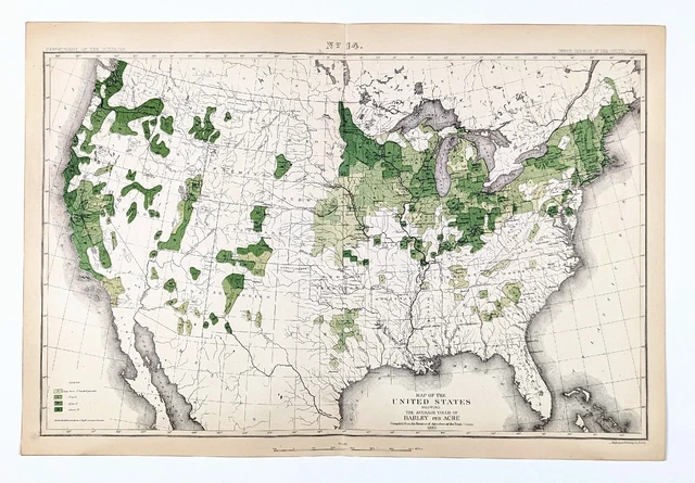
1880 UNITED STATES Map Barley Farming Agriculture Wisconsin California ...
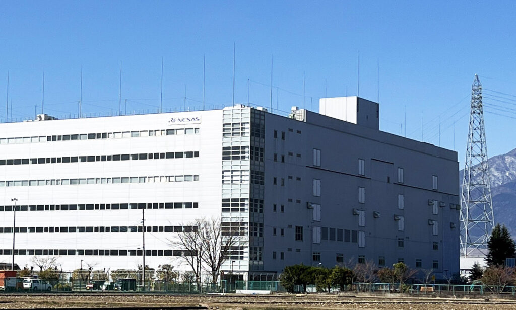
Renesas Boosts Power IC Yield with 300mm Kofu Plant | AEI
Defi Yield Farming: Risks and Rewards Part- 18
1880 UNITED STATES Map Barley Farming Agriculture Wisconsin California ...
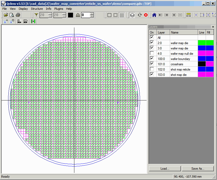
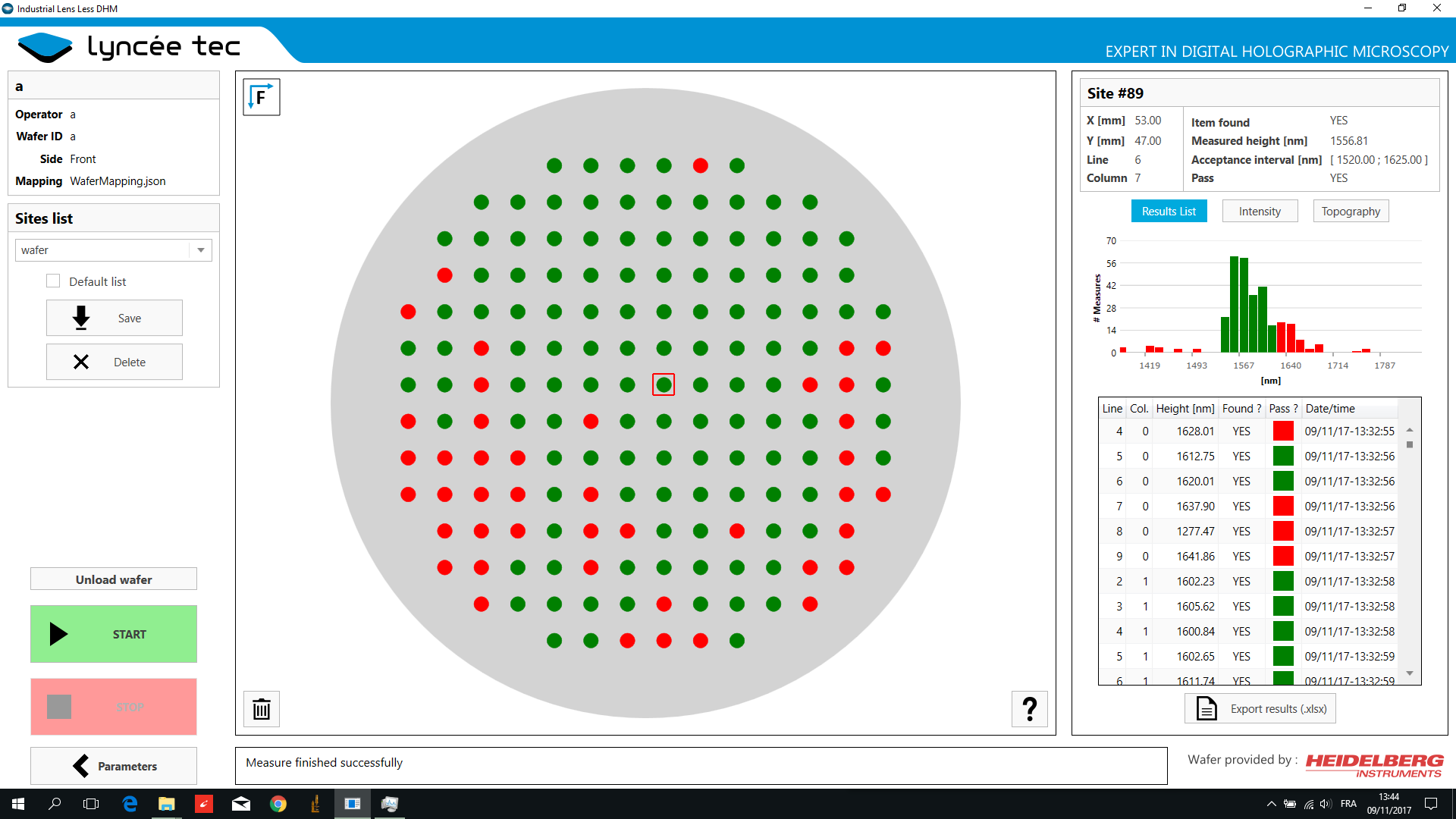
Wafer Mapping
Wafer Map Format
Wafer Defect Map
Wafer Bin Map
Wafer Test Map
300Mm Wafer
Wafer Heat Map
Silicon Wafer
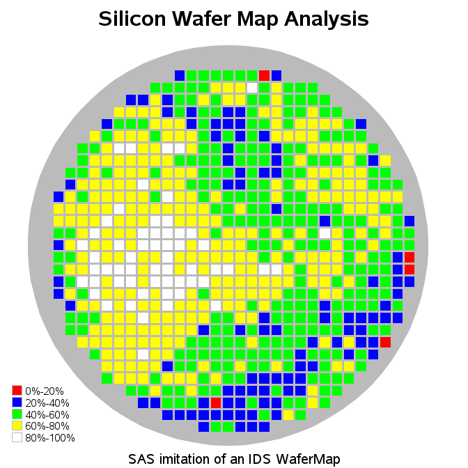
Wafer Map Analysis
Semiconductor Wafer Icon
Wafer Wat
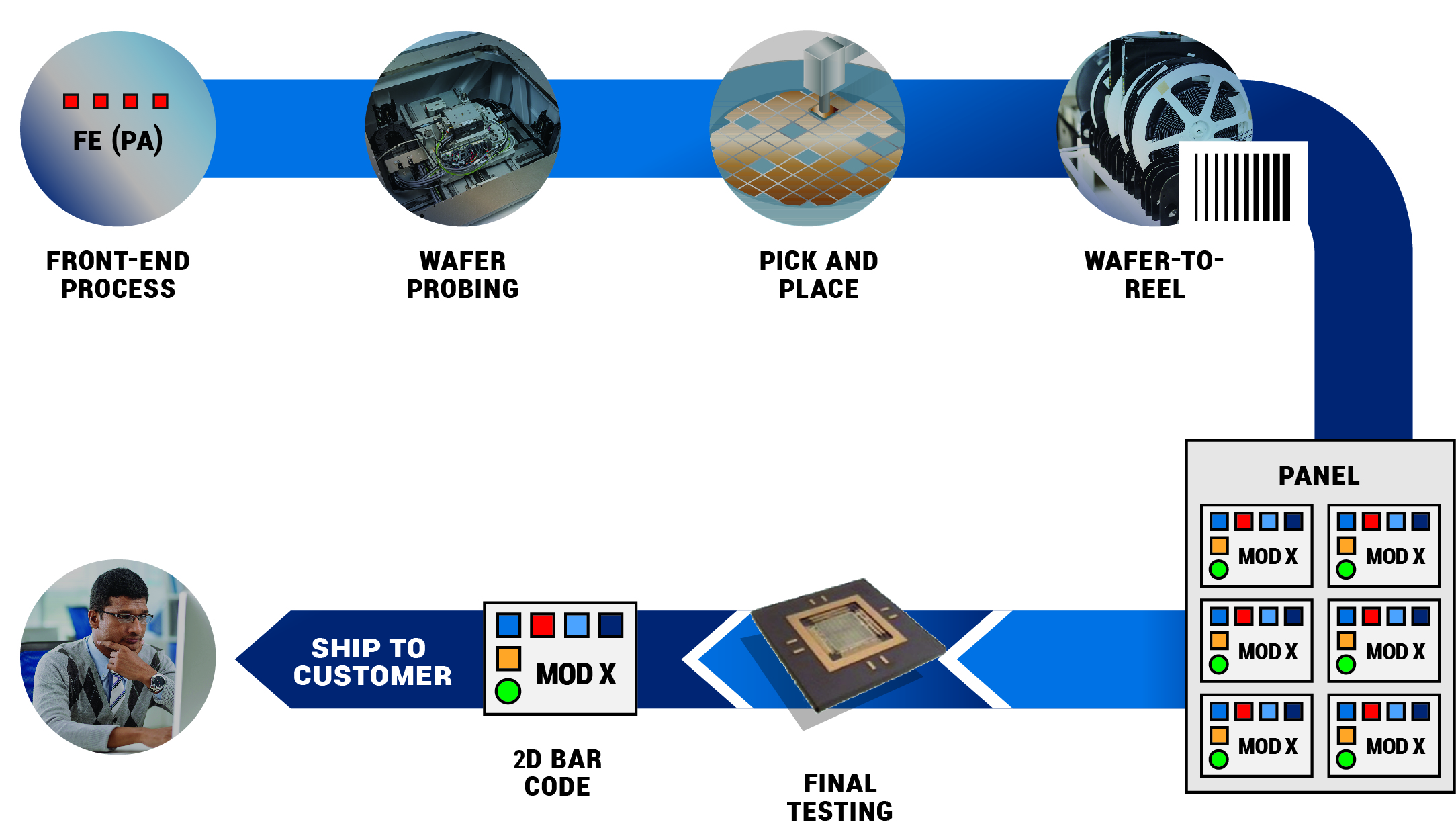
Wafer Manufacturing Process
Wafer Map Pattern
Wafer Shot Map
Excel Wafer Map
Wafer Map Data
Python Wafer Map
JMP Wafer Map
Wafer Map Spotfire


![Multi-year Experience with Yield Monitoring - [PPT Powerpoint]](https://reader035.vdocument.in/reader035/viewer/2022062310/56816096550346895dcfbea5/html5/thumbnails/1.jpg)


![Multi-year Experience with Yield Monitoring - [PPT Powerpoint]](https://reader035.vdocument.in/reader035/viewer/2022062310/56816096550346895dcfbea5/html5/thumbnails/3.jpg)