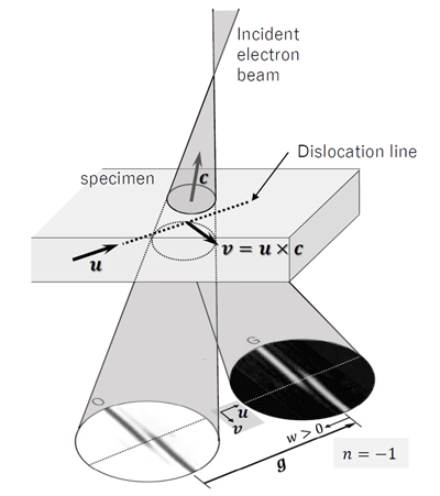
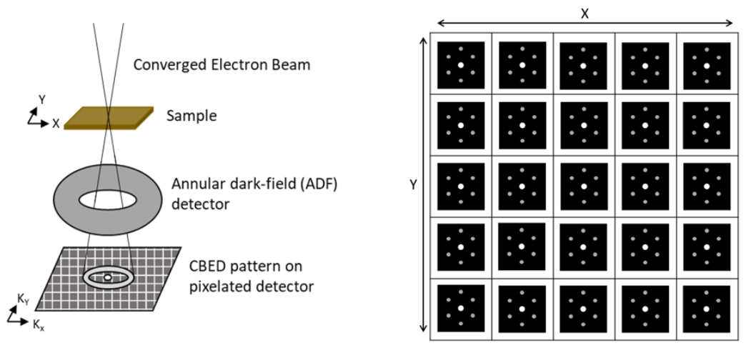
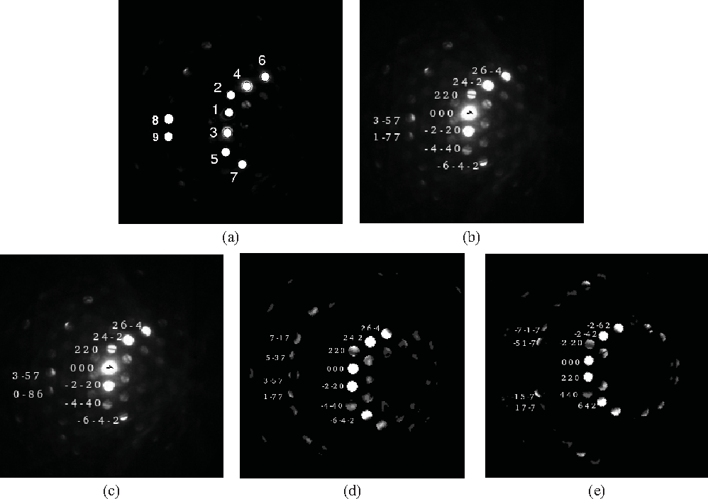
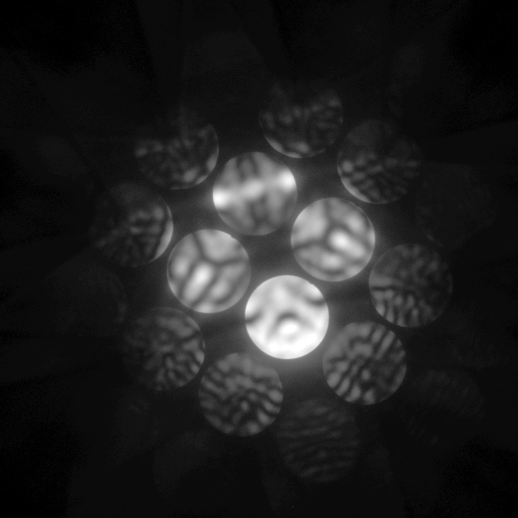
Tem Cbed Pattern


![(a) CBED pattern taken along [0001]; (b) CBED pattern recorded when the ...](https://www.researchgate.net/publication/257809473/figure/fig1/AS:614056994025474@1523414004540/a-CBED-pattern-taken-along-0001-b-CBED-pattern-recorded-when-the-sample-was-tilted.png)


![CBED pattern in the [110] direction of the triangular prismatic Au ...](https://www.researchgate.net/publication/353738621/figure/fig2/AS:11431281106541715@1670783606360/a-TEM-bright-field-image-of-a-triangular-prismatic-particle-with-b-690-nm-and-h-590_Q320.jpg)


![(a) Experimental CBED pattern of 6H-SiC [0001] at about 100kV and (b ...](https://www.researchgate.net/profile/Andreas-Fissel/publication/228819428/figure/fig1/AS:1053374623535104@1628155489254/Bright-field-images-of-heterostructures-grown-on-an-on-axis-a-4H-SiC-and-b-6H-SiC_Q640.jpg)

![Example - CBED pattern of bcc Fe [001]](https://pgi-jcns.fz-juelich.de/barthel/img/example-CBED-Results-alpha25mrad.png)


![Image and CBED patterns recorded from [ 1 1 ¯ 00 ]... | Download ...](https://www.researchgate.net/profile/Oliver-Bierwagen/publication/260309161/figure/download/fig2/AS:287879537414152@1445647240575/Image-and-CBED-patterns-recorded-from-1-1-00-cross-section-TEM-sample.png)


![(a) Sixteen CBED patterns from [110] silicon with varying beam tilts ...](https://www.researchgate.net/profile/Richard-Beanland/publication/239947083/figure/fig6/AS:393265590358023@1470773231618/a-SAED-b-CBED-and-c-montage-of-45-D-LACBED-patterns-taken-from-00-PC-NaBiCaTeO_Q640.jpg)

![CBED patterns for KNLNS0.07-BZ piezoceramic with [110] beam incidence ...](https://www.researchgate.net/profile/Jinghui-Gao-4/publication/276833181/figure/fig4/AS:282626280706053@1444394764497/CBED-patterns-for-KNLNS007-BZ-piezoceramic-with-110-beam-incidence-a2-shows-the.png)

![CBED measurements at the [110] zone axis a–d) and the [1¯10$\bar{1}10 ...](https://www.researchgate.net/publication/371291235/figure/fig3/AS:11431281166197506@1686204148533/CBED-measurements-at-the-110-zone-axis-a-d-and-the-110bar110-zone-axis-e-h.png)


![TEM image of a nucleation island acquired along the [11-20] zone axis ...](https://www.researchgate.net/profile/Pierre-Marie-Coulon/publication/262643235/figure/fig3/AS:289019293388835@1445918977662/TEM-image-of-a-nucleation-island-acquired-along-the-11-20-zone-axis-Inset-CBED.png)


![Image and CBED patterns recorded from [ 1 1 ¯ 00 ]... | Download ...](https://www.researchgate.net/profile/Oliver-Bierwagen/publication/260309161/figure/fig3/AS:289017414340652@1445918529880/Color-online-Comparison-of-surface-morphology-of-UID-top-left-and-Mg-doped-InN-with_Q640.jpg)


![(a) TEM BF image from the [100] axis of the cross-section through the ...](https://www.researchgate.net/profile/W-bill-Clegg/publication/235623877/figure/fig3/AS:347060277661706@1459757027055/a-TEM-BF-image-from-the-100-axis-of-the-cross-section-through-the-indentation-in-MgO.png)


![CBED patterns in the [111] direction of the triangular prismatic Au ...](https://www.researchgate.net/publication/353738621/figure/fig4/AS:11431281106567580@1670783606621/a-TEM-bright-field-image-of-a-triangular-prismatic-Au-particle-with-b-10-m-and-h_Q320.jpg)

![(a) TEM BF image from the [100] axis of the cross-section through the ...](https://www.researchgate.net/profile/W-bill-Clegg/publication/235623877/figure/fig2/AS:347060277661705@1459757026881/a-TEM-BF-image-from-the-100-axis-of-the-cross-section-through-the-indentation-in-Cu.png)


![50 nm specimen thickness, [100]-Si convergent beam electron diffraction ...](https://www.researchgate.net/publication/370836755/figure/fig2/AS:11431281159406095@1684345420199/50-nm-specimen-thickness-100-Si-convergent-beam-electron-diffraction-CBED-patterns.png)

Access our comprehensive Tem Cbed Pattern database featuring extensive collections of professionally captured photographs. enhanced through professional post-processing for maximum visual impact. meeting the demanding requirements of professional projects. Discover high-resolution Tem Cbed Pattern images optimized for various applications. Perfect for marketing materials, corporate presentations, advertising campaigns, and professional publications All Tem Cbed Pattern images are available in high resolution with professional-grade quality, optimized for both digital and print applications, and include comprehensive metadata for easy organization and usage. Each Tem Cbed Pattern image meets rigorous quality standards for commercial applications. Professional licensing options accommodate both commercial and educational usage requirements. Comprehensive tagging systems facilitate quick discovery of relevant Tem Cbed Pattern content. Multiple resolution options ensure optimal performance across different platforms and applications. Reliable customer support ensures smooth experience throughout the Tem Cbed Pattern selection process. The Tem Cbed Pattern collection represents years of careful curation and professional standards. Instant download capabilities enable immediate access to chosen Tem Cbed Pattern images. Whether for commercial projects or personal use, our Tem Cbed Pattern collection delivers consistent excellence. Diverse style options within the Tem Cbed Pattern collection suit various aesthetic preferences. Advanced search capabilities make finding the perfect Tem Cbed Pattern image effortless and efficient.