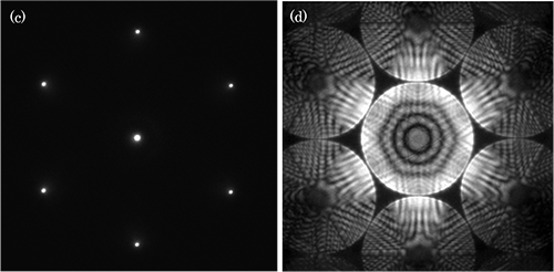
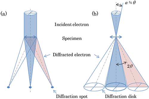
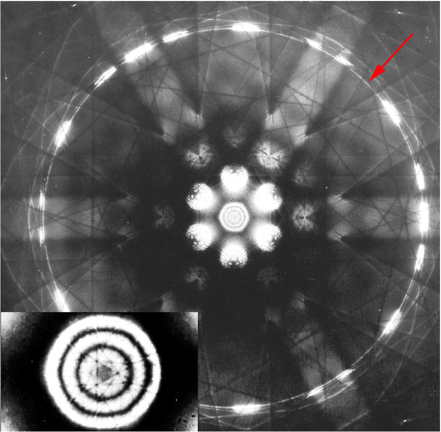
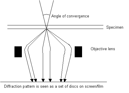
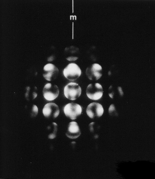
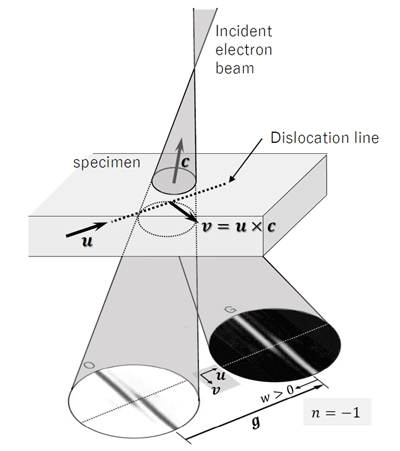
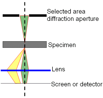
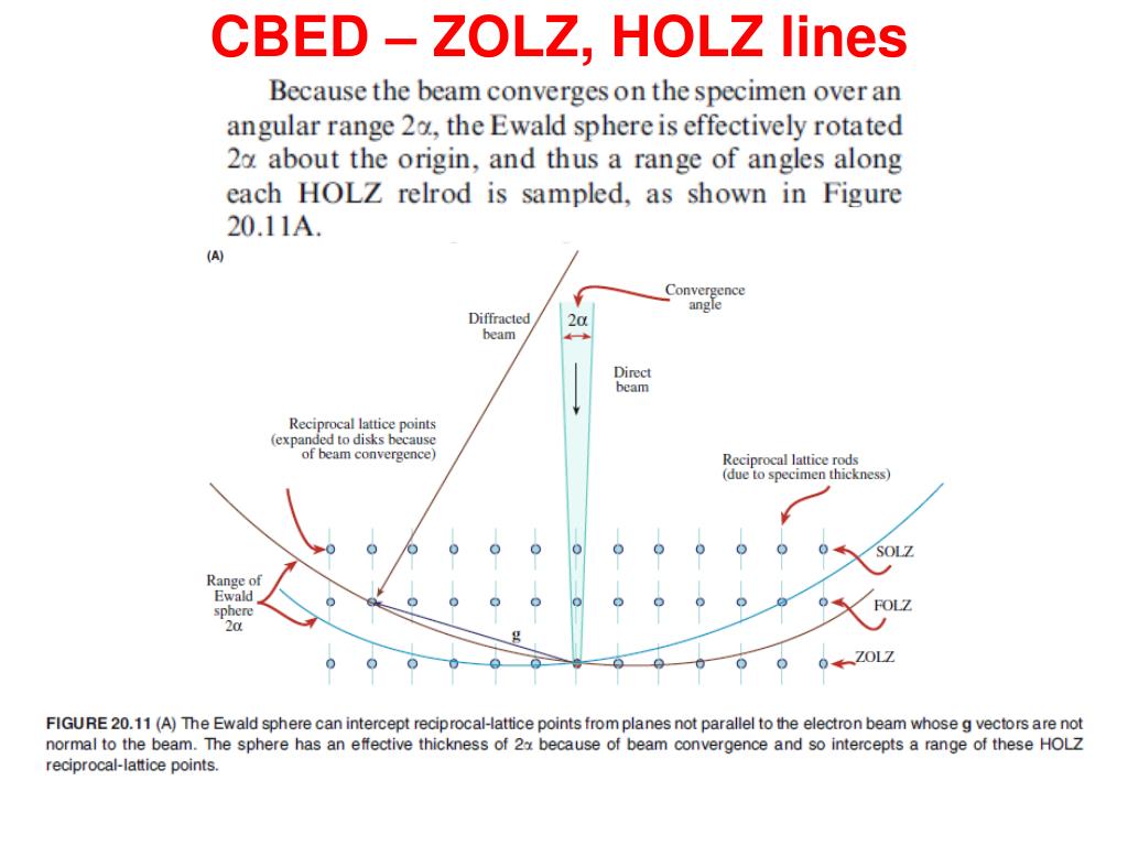
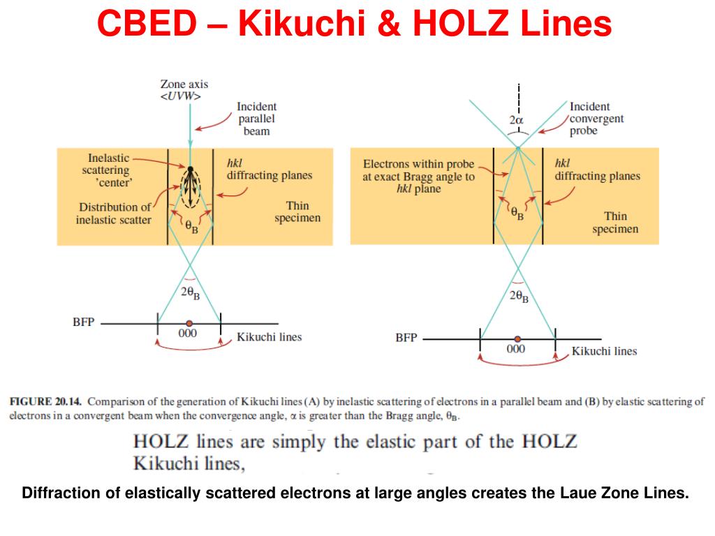
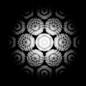
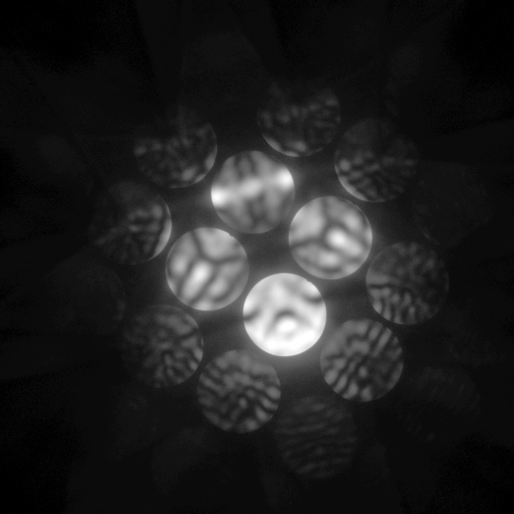
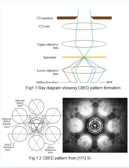
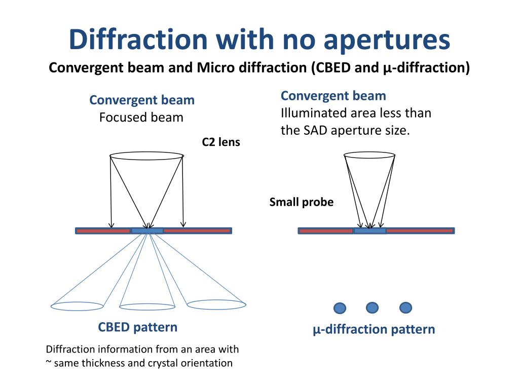
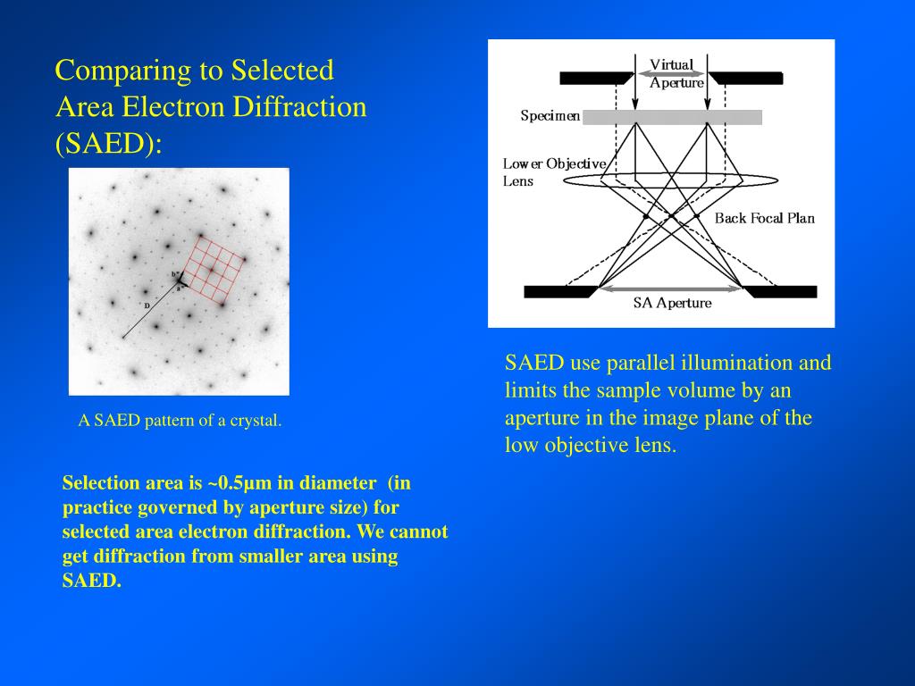
Cbed Diffraction
![CBED diffraction patterns in the [0 0 1] crystal direction at different ...](https://www.researchgate.net/profile/Rainer-Schmidt-2/publication/277592562/figure/fig3/AS:281877601636354@1444216265700/CBED-diffraction-patterns-in-the-0-0-1-crystal-direction-at-different-camera-constants.png)


![CBED diffraction patterns in the [0 0 1] crystal direction at different ...](https://www.researchgate.net/profile/Rainer-Schmidt-2/publication/277592562/figure/fig3/AS:281877601636354@1444216265700/CBED-diffraction-patterns-in-the-0-0-1-crystal-direction-at-different-camera-constants_Q320.jpg)


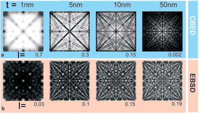
![50 nm specimen thickness, [100]-Si convergent beam electron diffraction ...](https://www.researchgate.net/publication/370836755/figure/fig2/AS:11431281159406095@1684345420199/50-nm-specimen-thickness-100-Si-convergent-beam-electron-diffraction-CBED-patterns.png)


![(a) CBED pattern taken along [0001]; (b) CBED pattern recorded when the ...](https://www.researchgate.net/publication/257809473/figure/fig1/AS:614056994025474@1523414004540/a-CBED-pattern-taken-along-0001-b-CBED-pattern-recorded-when-the-sample-was-tilted.png)

![[1T00] CBED patterns of TI crystals. (a) Whole pattern and (b ...](https://www.researchgate.net/profile/Kenneth-Vecchio/publication/251394196/figure/fig5/AS:668963113533456@1536504643649/1T00-CBED-patterns-of-TI-crystals-a-Whole-pattern-and-b-projection-diffraction_Q640.jpg)
![(a) Sixteen CBED patterns from [110] silicon with varying beam tilts ...](https://www.researchgate.net/profile/Richard-Beanland/publication/239947083/figure/fig1/AS:393265586163714@1470773230783/a-The-geometry-of-large-angle-convergent-beam-electron-diffraction-LACBED-for-one_Q640.jpg)


![(a) Sixteen CBED patterns from [110] silicon with varying beam tilts ...](https://www.researchgate.net/profile/Richard-Beanland/publication/239947083/figure/fig6/AS:393265590358023@1470773231618/a-SAED-b-CBED-and-c-montage-of-45-D-LACBED-patterns-taken-from-00-PC-NaBiCaTeO_Q640.jpg)

![[0001] CBED patterns of T 1 crystals. (a) Whole pattern and (b ...](https://www.researchgate.net/profile/Kenneth-Vecchio/publication/251394196/figure/fig4/AS:668963113545745@1536504643559/0001-CBED-patterns-of-T-1-crystals-a-Whole-pattern-and-b-projection-diffraction_Q320.jpg)


![CBED patterns taken at [010] incidence from SBN (x =0.32) at 573 K from ...](https://www.researchgate.net/profile/Bikas-Aryal-2/publication/332385372/figure/fig1/AS:748240974667777@1555405958525/CBED-patterns-taken-at-010-incidence-from-SBN-x-032-at-573-K-from-a-the-first.jpg)


![a) [100] and (b) [001] CBED patterns recorded from d phase. | Download ...](https://www.researchgate.net/profile/Xiaojun-Zhao-12/publication/337806094/figure/fig4/AS:836651215511552@1576484602085/a-100-and-b-001-CBED-patterns-recorded-from-d-phase_Q640.jpg)


![CBED patterns in the [111] direction of the triangular prismatic Au ...](https://www.researchgate.net/publication/353738621/figure/fig5/AS:11431281106593458@1670783607184/CBED-patterns-in-the-111-direction-of-the-triangular-prismatic-Au-particle-shown-in_Q640.jpg)
![50 nm specimen thickness, [100]-Si convergent beam electron diffraction ...](https://www.researchgate.net/publication/370836755/figure/fig3/AS:11431281159378242@1684345420654/Phonon-phase-scrambling-algorithm-PSA-simulation-results-for-the-convergent-beam_Q320.jpg)

![a) [100] and (b) [001] CBED patterns recorded from d phase. | Download ...](https://www.researchgate.net/publication/337806094/figure/fig4/AS:836651215511552@1576484602085/a-100-and-b-001-CBED-patterns-recorded-from-d-phase.png)


![CBED patterns for KNLNS0.07-BZ piezoceramic with [110] beam incidence ...](https://www.researchgate.net/profile/Jinghui-Gao-4/publication/276833181/figure/fig4/AS:282626280706053@1444394764497/CBED-patterns-for-KNLNS007-BZ-piezoceramic-with-110-beam-incidence-a2-shows-the.png)

![Example - CBED pattern of bcc Fe [001]](https://pgi-jcns.fz-juelich.de/barthel/img/example-CBED-Results-alpha25mrad.png)

![CBED patterns taken along (a) fivefold [10], (b) threefold [111] and ...](https://www.researchgate.net/profile/Leonid-Bendersky/publication/237271139/figure/fig7/AS:668562561720323@1536409144185/CBED-patterns-taken-along-a-fivefold-10-b-threefold-111-and-c-twofold-001_Q640.jpg)


![Example - CBED pattern of bcc Fe [001]](https://pgi-jcns.fz-juelich.de/barthel/img/example-CBED-Results-alpha5mrad-tilt.png)


+is+a+powerful+tool+for+analysing+and+identifying+symmetry+in+materials..jpg)


Experience the unique perspectives of Cbed Diffraction with our abstract gallery of comprehensive galleries of images. featuring creative examples of photography, images, and pictures. designed to inspire imagination and creativity. Each Cbed Diffraction image is carefully selected for superior visual impact and professional quality. Suitable for various applications including web design, social media, personal projects, and digital content creation All Cbed Diffraction images are available in high resolution with professional-grade quality, optimized for both digital and print applications, and include comprehensive metadata for easy organization and usage. Discover the perfect Cbed Diffraction images to enhance your visual communication needs. Diverse style options within the Cbed Diffraction collection suit various aesthetic preferences. Reliable customer support ensures smooth experience throughout the Cbed Diffraction selection process. Comprehensive tagging systems facilitate quick discovery of relevant Cbed Diffraction content. Whether for commercial projects or personal use, our Cbed Diffraction collection delivers consistent excellence. Time-saving browsing features help users locate ideal Cbed Diffraction images quickly. Professional licensing options accommodate both commercial and educational usage requirements. The Cbed Diffraction archive serves professionals, educators, and creatives across diverse industries. Cost-effective licensing makes professional Cbed Diffraction photography accessible to all budgets. Advanced search capabilities make finding the perfect Cbed Diffraction image effortless and efficient.