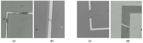
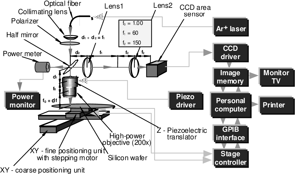
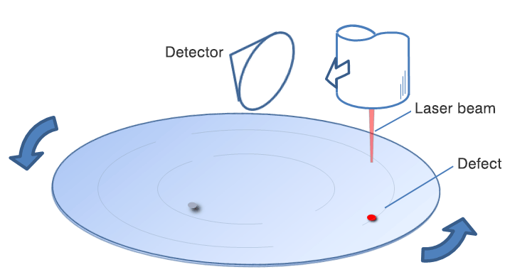
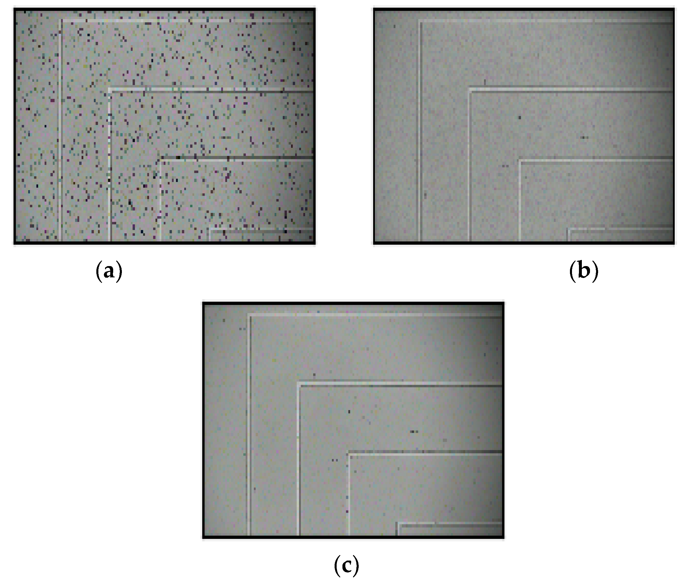
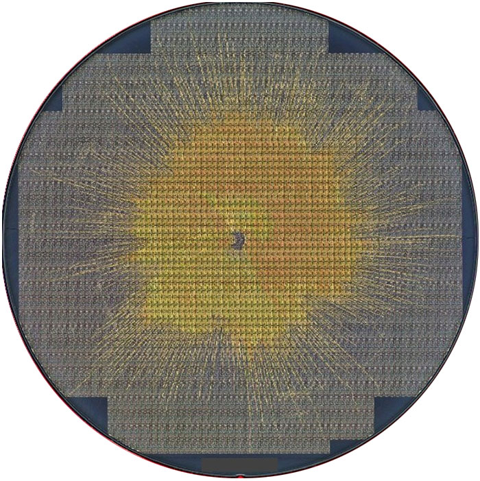
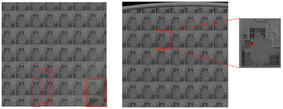
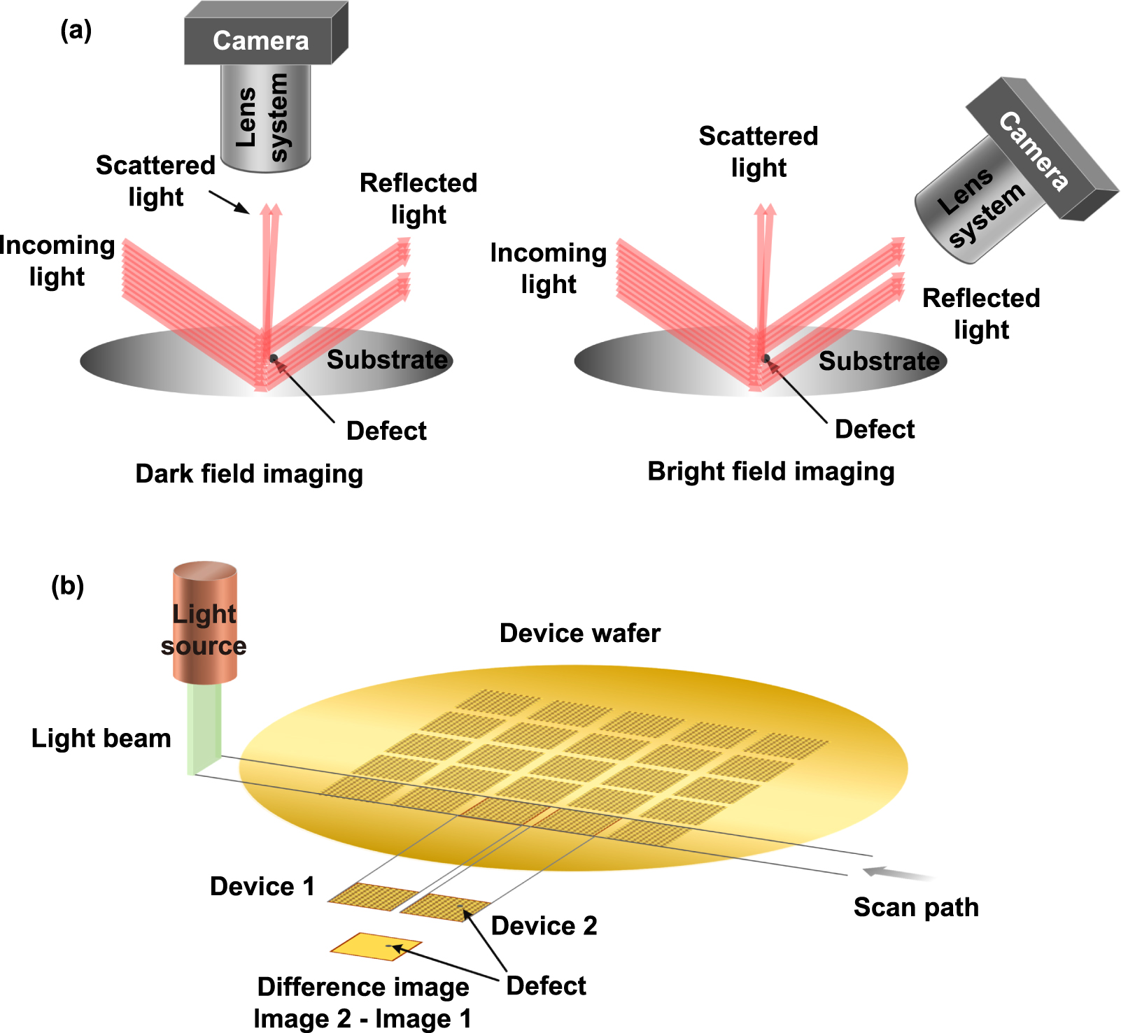
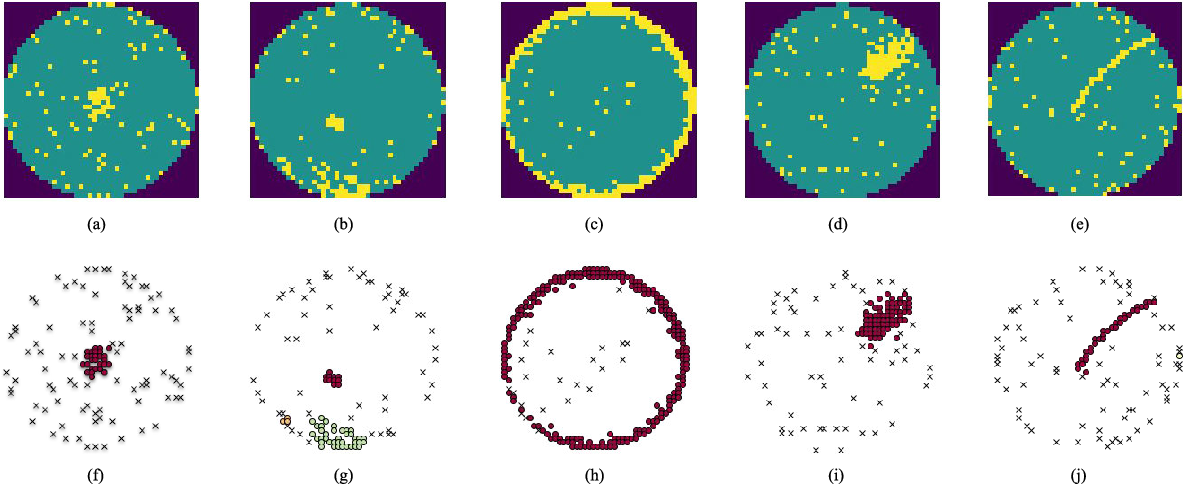
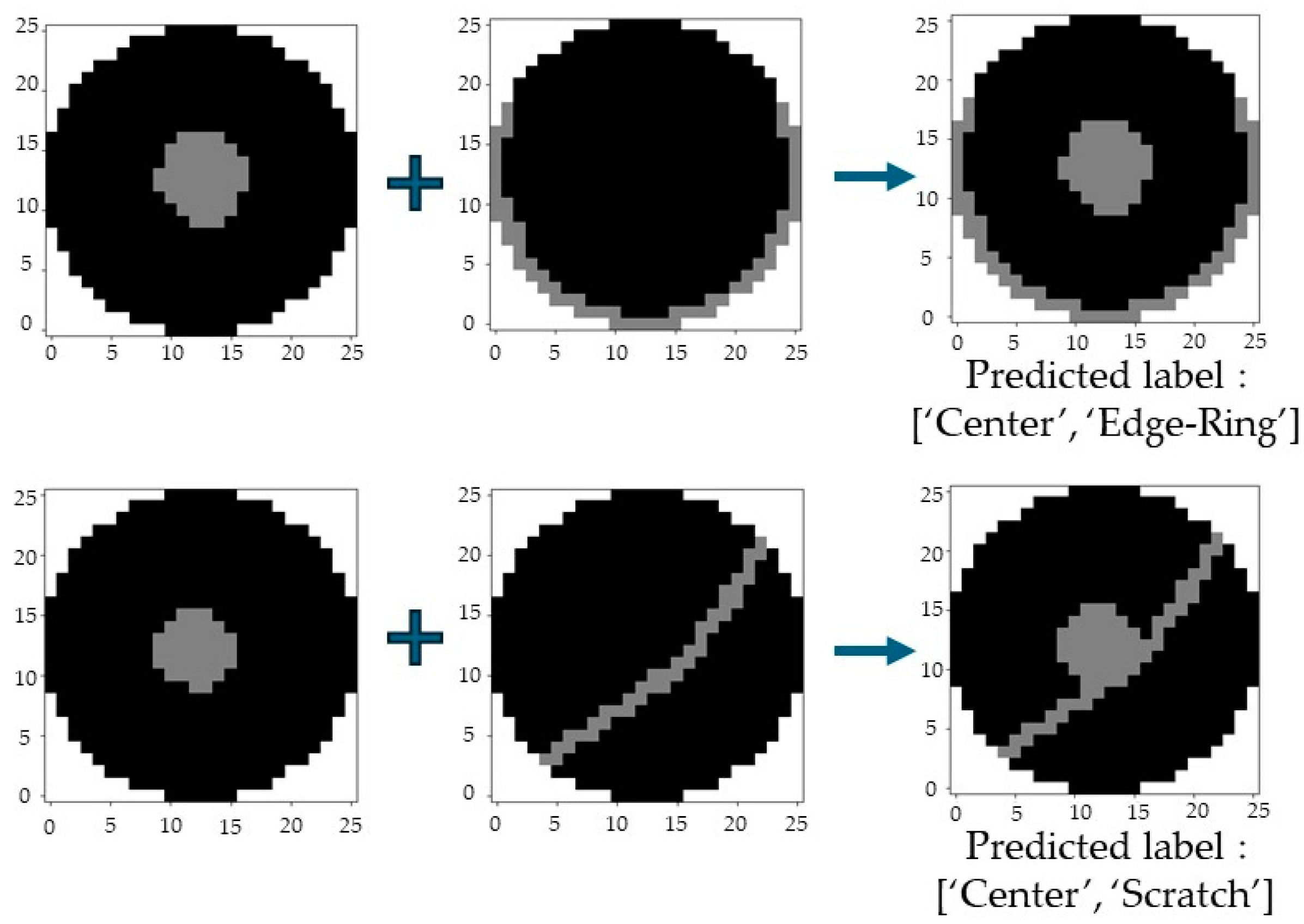
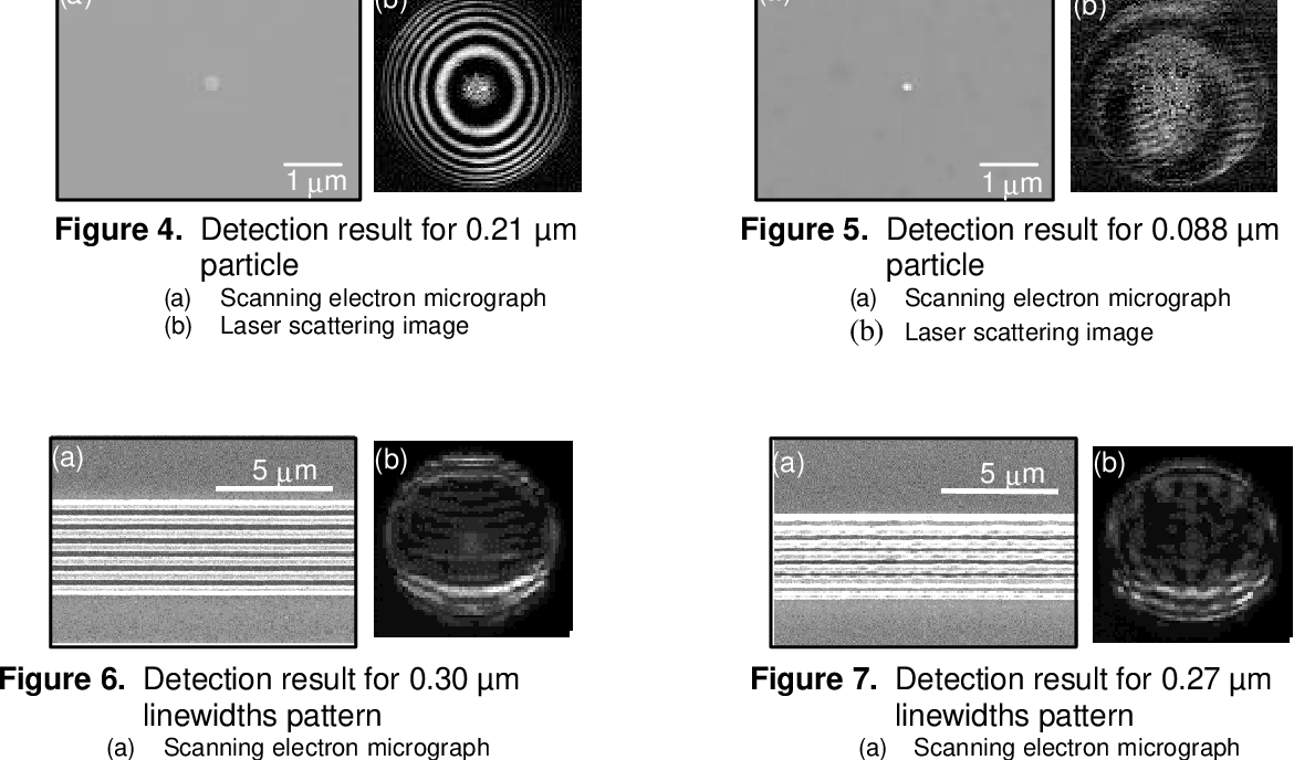
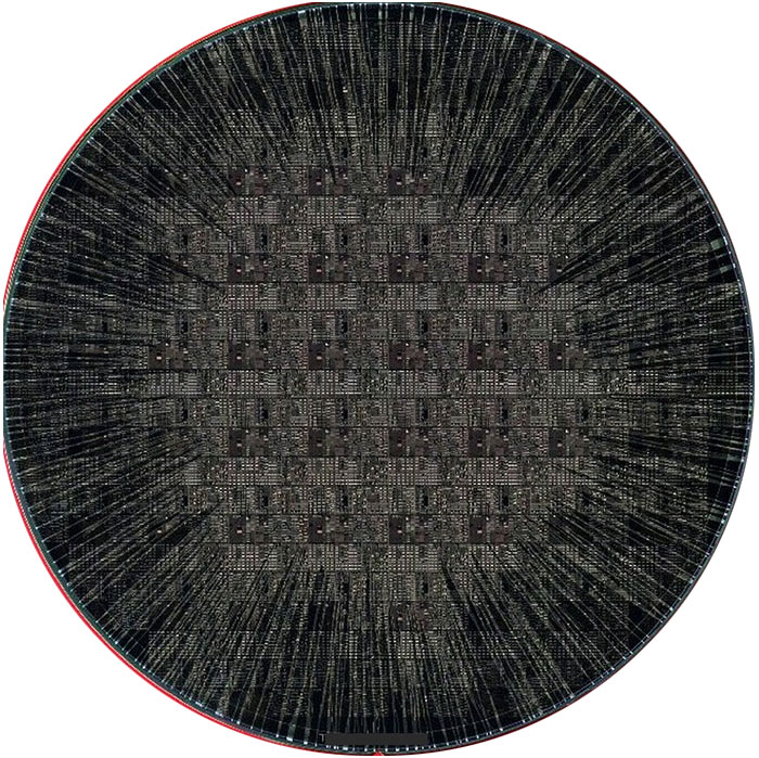
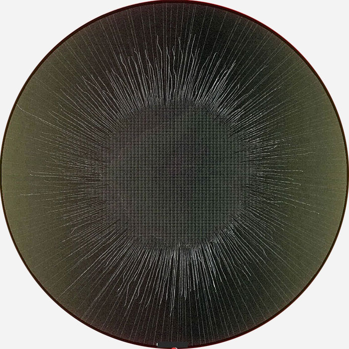
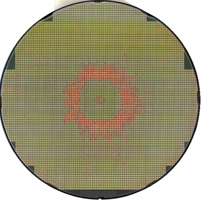
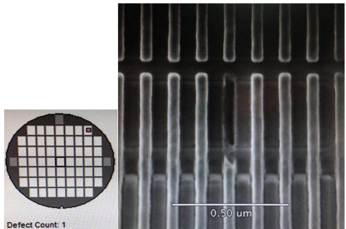
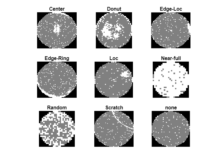
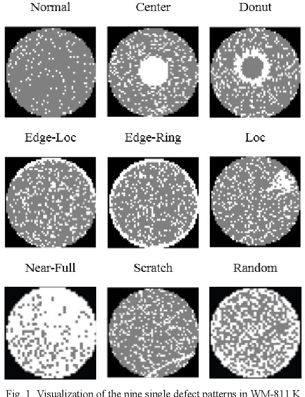
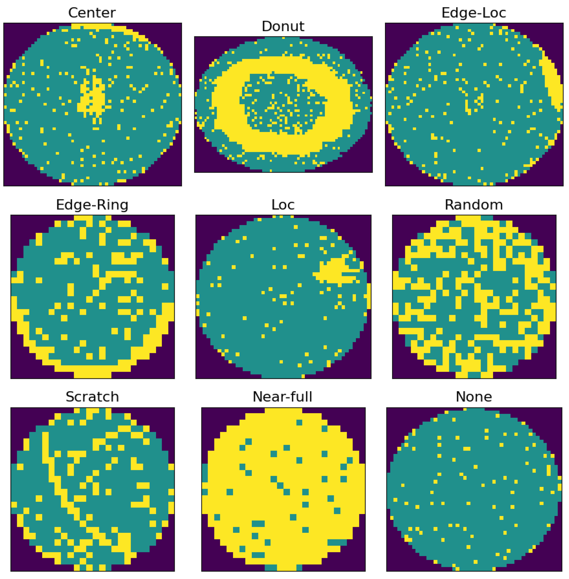
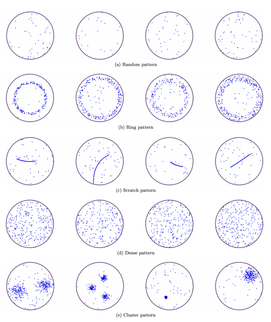
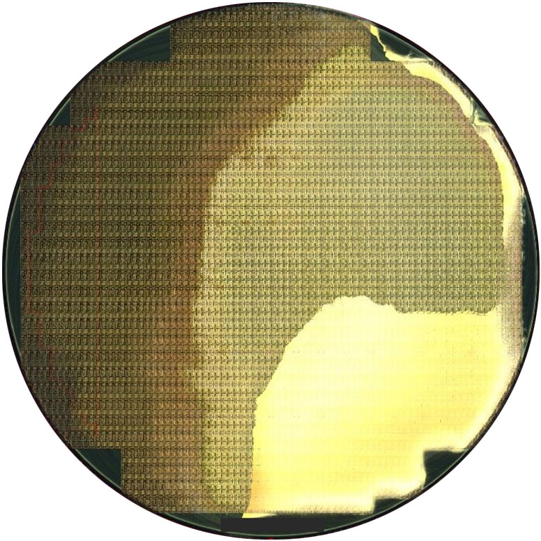
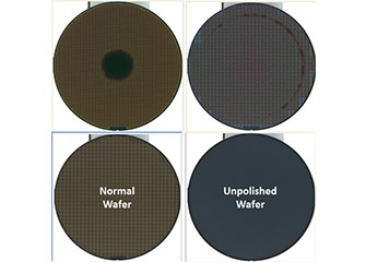
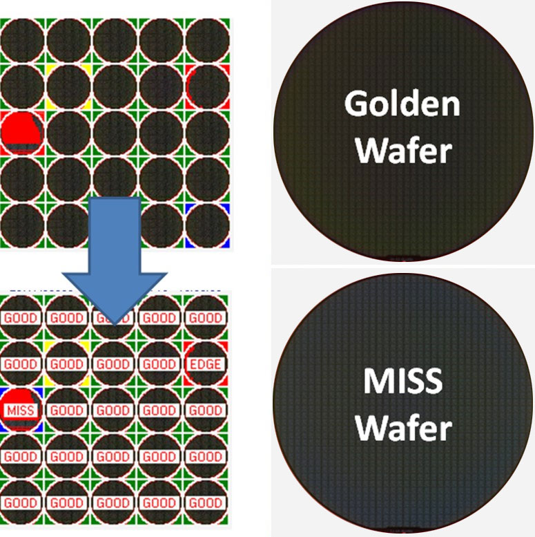
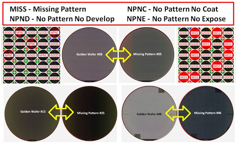
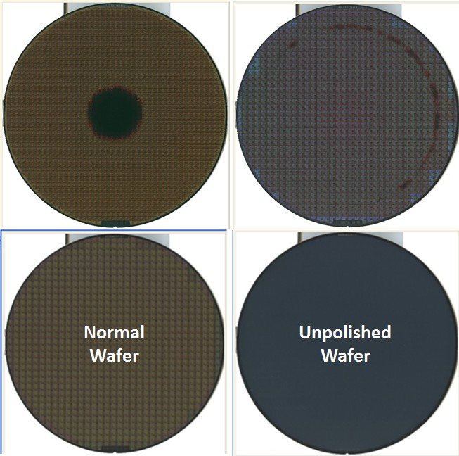
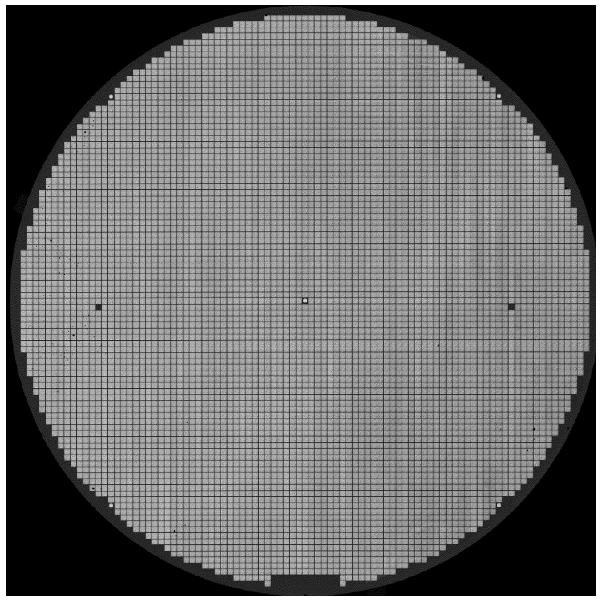
Patterned Wafer Defect


![[PDF] Wafer Map Failure Pattern Recognition and Similarity Ranking for ...](https://d3i71xaburhd42.cloudfront.net/a581566276f3b2242ec6544c185204a96f17db8a/3-Figure2-1.png)


Drive innovation with our technology Patterned Wafer Defect gallery of hundreds of digital images. innovatively presenting photography, images, and pictures. ideal for innovation showcases and presentations. Browse our premium Patterned Wafer Defect gallery featuring professionally curated photographs. Suitable for various applications including web design, social media, personal projects, and digital content creation All Patterned Wafer Defect images are available in high resolution with professional-grade quality, optimized for both digital and print applications, and include comprehensive metadata for easy organization and usage. Discover the perfect Patterned Wafer Defect images to enhance your visual communication needs. Reliable customer support ensures smooth experience throughout the Patterned Wafer Defect selection process. Professional licensing options accommodate both commercial and educational usage requirements. Cost-effective licensing makes professional Patterned Wafer Defect photography accessible to all budgets. The Patterned Wafer Defect collection represents years of careful curation and professional standards. The Patterned Wafer Defect archive serves professionals, educators, and creatives across diverse industries. Instant download capabilities enable immediate access to chosen Patterned Wafer Defect images. Our Patterned Wafer Defect database continuously expands with fresh, relevant content from skilled photographers. Whether for commercial projects or personal use, our Patterned Wafer Defect collection delivers consistent excellence. Diverse style options within the Patterned Wafer Defect collection suit various aesthetic preferences.