Please enter url.
Login
Logout
Please enter url.
(a) DRAM cube on substrate, (b) X-ray image of 4-layer DRAM cube Figure ...
researchgate.net
source
Comments
Different TSV integration process flow | Download Scientific Diagram
3-D self-assembled MEMS: a) flow sensor, b) thermal actuator ...
Failure modes of the MEMS structures: a) fractured comb arms, c ...
NEMS switches using ohmic contact (a) and using capacitive contact (b ...
Failure modes of the MEMS comb structure. (a) Top view of the ...
SEM images of the etching profile angles obtained with different ...
(PDF) Dynamic control of the asymmetric Fano resonance in side-coupled ...
Cross-sectional SEM images of thick copper wires surrounded by CoZrTa ...
SEM images of the fabricated switches: a Plan view of a switch D1. The ...
(a) XPS Si 2p spectra and (b) XPS O 1s spectra of Si NWs before and ...
EES
3-D self-assembled MEMS: a) flow sensor, b) thermal actuator ...
Relationship of the magnetic flux density and the gap distance between ...
͑ a ͒ Scanning electron microscopy image of the magneto-transport ...
XRD patterns of the Sb2Se3 NWs and Sb2Se3 standard (Joint Committee on ...
Micromachines | Free Full-Text | Mechanically-Tunable Photonic Devices ...
FIB-SEM tomography analyzed volume: (a) image showing 52° cross-section ...
FIB pictures of (a) top and (b) front view of fourth-order gratings ...
Table 4 from Development of 3D Thin WLCSP Using Vertical Via Last TSV ...
Very Large Scale Integration (VLSI): Intel’s e-DRAM
(PDF) Impact of through silicon via induced mechanical stress on fully ...
Figure 1 from A noble VFO(Vertical wire Fan Out) technology for small ...
Anna FONTCUBERTA I MORRAL | Professor (Full) | Full Professor | École ...
Interfaces to Neuronal Networks | Centre for Nano Science and ...
Representative metallographic microscope photographs of the solder ...
Sensoric Micro and Nano Systems: physica status solidi (a): Vol 216, No 19
Proposed failure mechanism of AuAl Kirkendall micro voiding and caused ...
Figure 10 from Via Processing Effects on Electromigration in 65 nm ...
Analysis of In electrodeposit saturated with antimony above the InSb ...
(a) Schematic of cross sectional view of the device along the waveguide ...
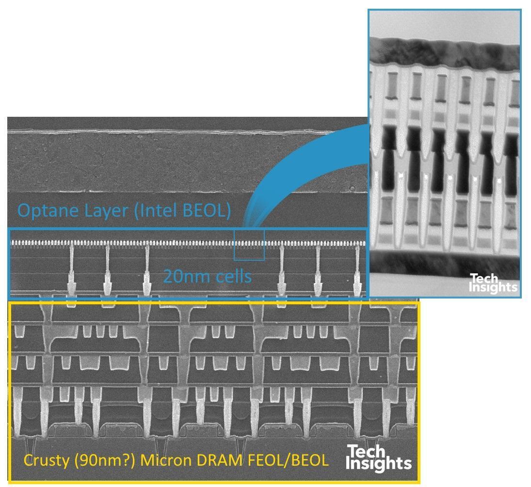
Micron Conspires With The Rest Of The Industry (NASDAQ:INTC) | Seeking ...
Cross-sectional scanning electron microscope (SEM) images of a portion ...
An Introduction to Micro System Analyzers in MEMS Laboratories
Atomically Thin Memristors - Hybrid 2D/CMOS Microchips for Memristive ...
REATISS: Capabilities Gallery
Dram-Layout
Dram-Memory-Cell
SRAM-Dram
Dram-Cell-Array
Dram-Capacitor
Dram-Cell-Structure
TSV-Dram
1T-Dram
Micron-Dram
3D-Dram-Samsung
Dram-Architecture
Dynamic-RAM-Dram
Stacked-Dram
Dram-Semiconductor
4F2-6F2
Dram-Cross-Section


.jpg)