Please enter url.
Login
Logout
Please enter url.
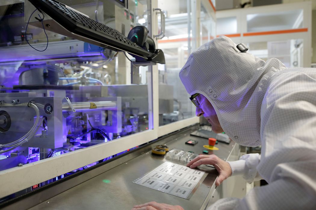
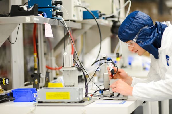
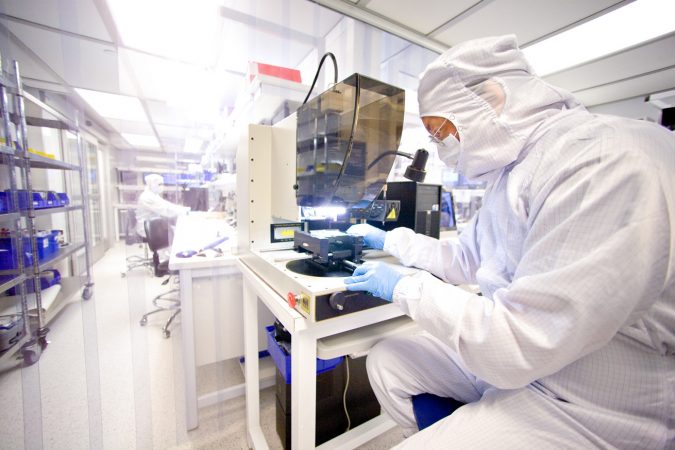
Smart Multilayer AlN Substrate and Packaging | TDK Electronics - TDK Europe
tdk-electronics.tdk.com
source
Comments
Smart Multilayer AlN Substrate and Packaging | TDK Electronics - TDK Europe
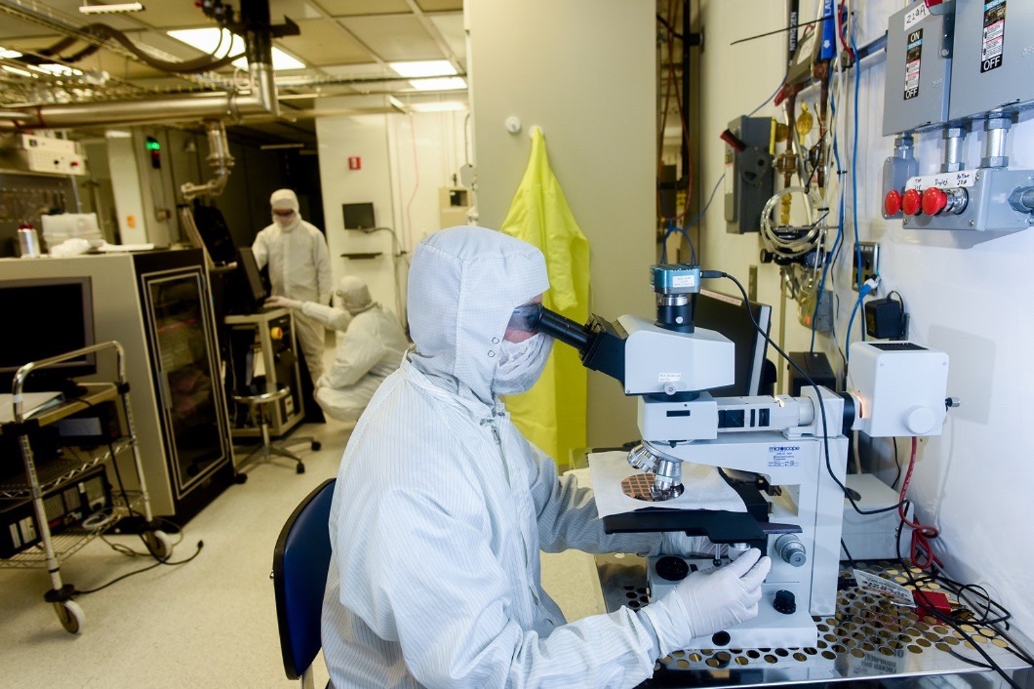
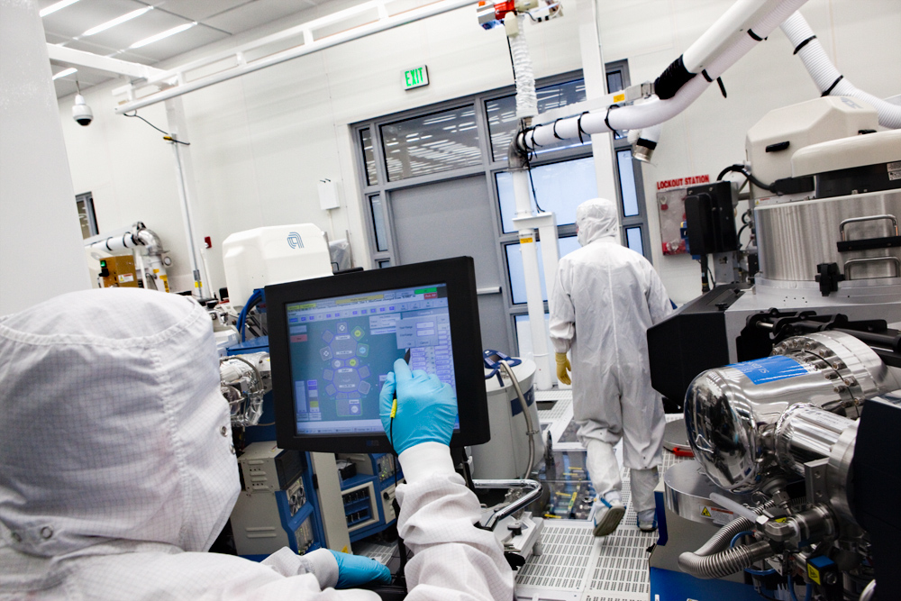
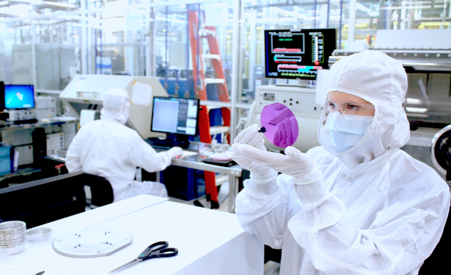
Image Gallery - Melbourne Centre for Nanofabrication
Biomedical Imaging & Spectroscopy | Biological Engineering and Small ...
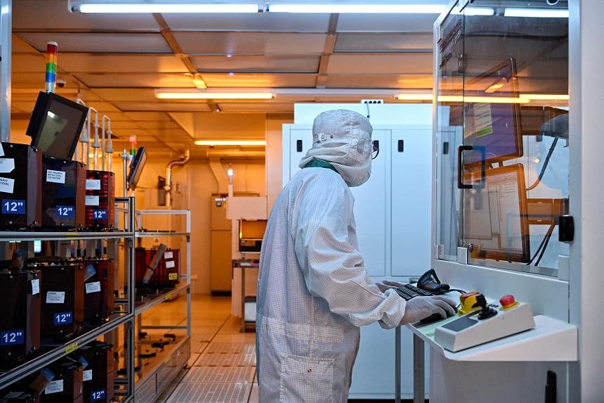
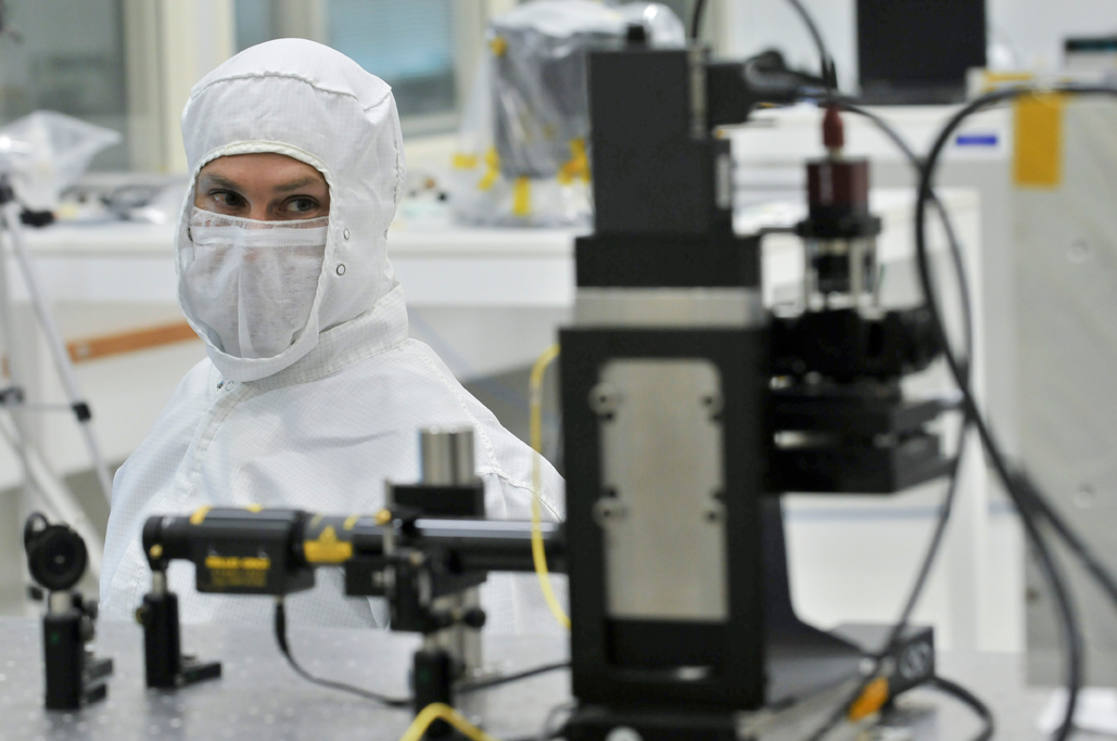
LASER - World of PHOTONICS 2022: Laser Development | Laser Zentrum Hannover
Study Michigan - Study at Michigan Colleges, Scholarships for ...
FDA Initiatives Drive 21st Century Advanced Manufacturing Technologies ...
Quick Turn Prototyping | Extrusions, Catheters, and Additive ...
Vaccine Dreams and Russian Reality | Think Global Health
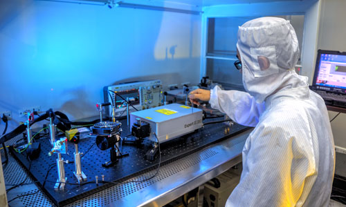
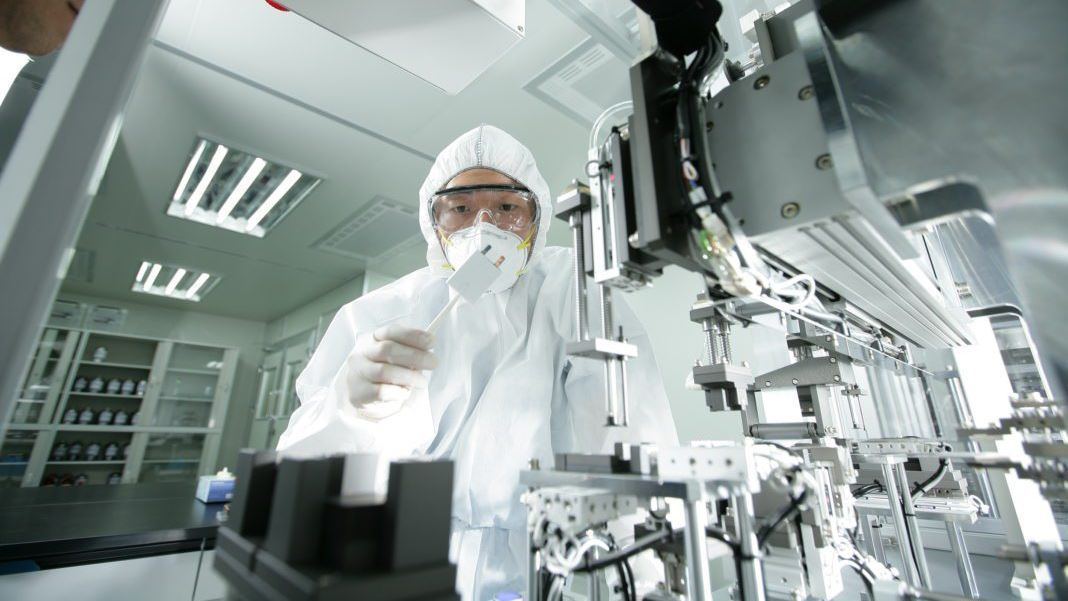
Advanced lithography - 4D LABS - Simon Fraser University
Taiyo Nippon Sanso and North Carolina State University Agree to Three ...
Samsung ready for mass production of micro LED displays
Samsung to launch 30-millimetre-thick luxury MicroLED TV next year | ZDNET
S’pore’s manufacturing, services sectors still positive despite ...
UV Laser 355nm 3W 5W 10W,green Laser 532nm,nanosecond Lasers,solid ...
EPSRC research outcomes and impact – UKRI
Managing Manufacturing | Business and Technology Magazine
Top 10 Best Hard Drive Recovery Services In The USA
Nanotechnology Systems - NAIT
4 Quality Management Tips For The Medical Device Industry - Welp Magazine
NASA's Stardust mission may have recovered first interstellar particles
Ford Plays The Long Game As EVs May Wait For 'Breakthrough' Moment
Egyptian Elham Fadaly Wins Physics World 2020 Breakthrough of the Year ...
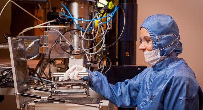
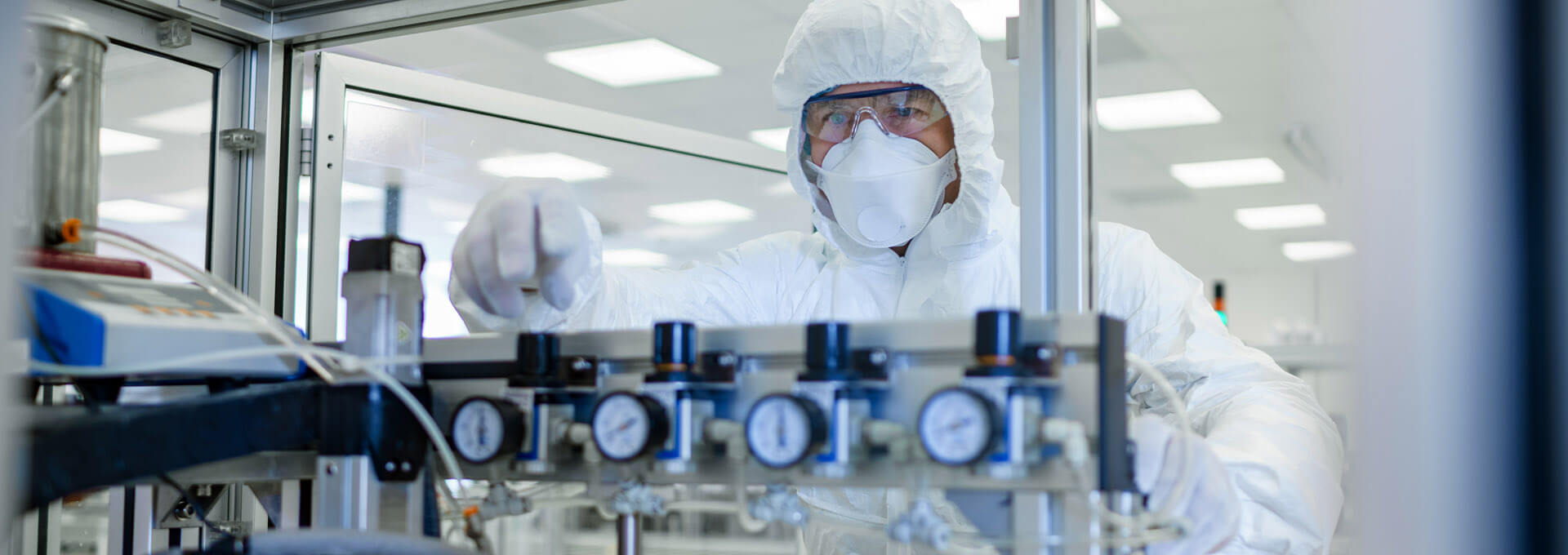
Piezo Solutions | TDK Electronics - TDK Europe
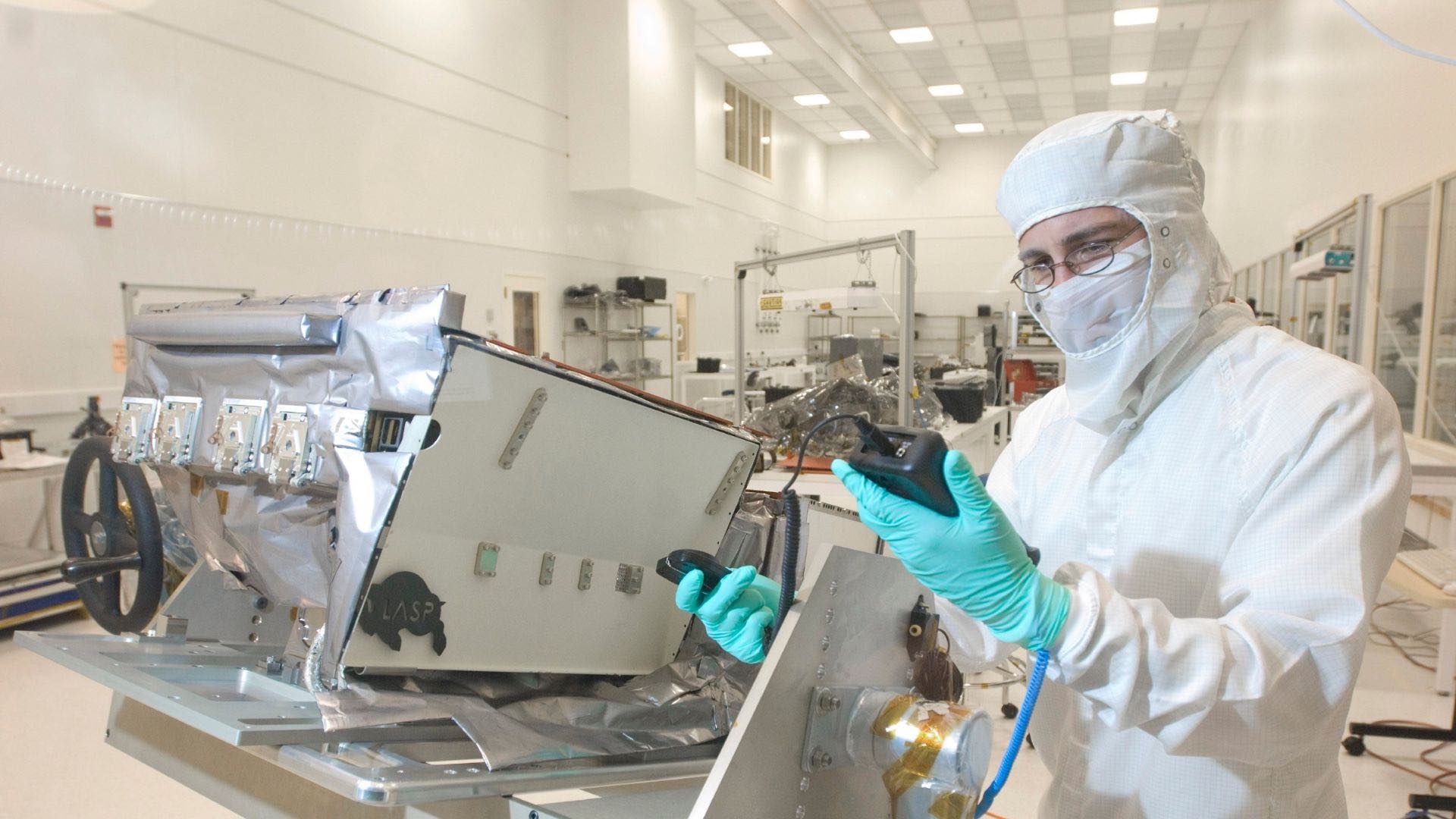
Mechanical Engineering - Laboratory for Atmospheric and Space Physics
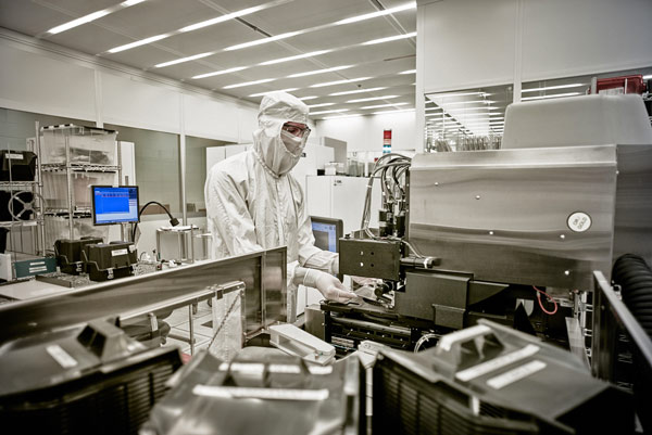
Facilities | Teledyne Imaging
Chemicals and materials to play key role in chips as 2-nm milestone ...
Materials Science and Engineering at the University of Delaware
Factors Affecting the Data Center Industry in 2023 - High-Tech Electrics
GM & POSCO Chemical to Invest $327 Million in Canadian Battery Material ...
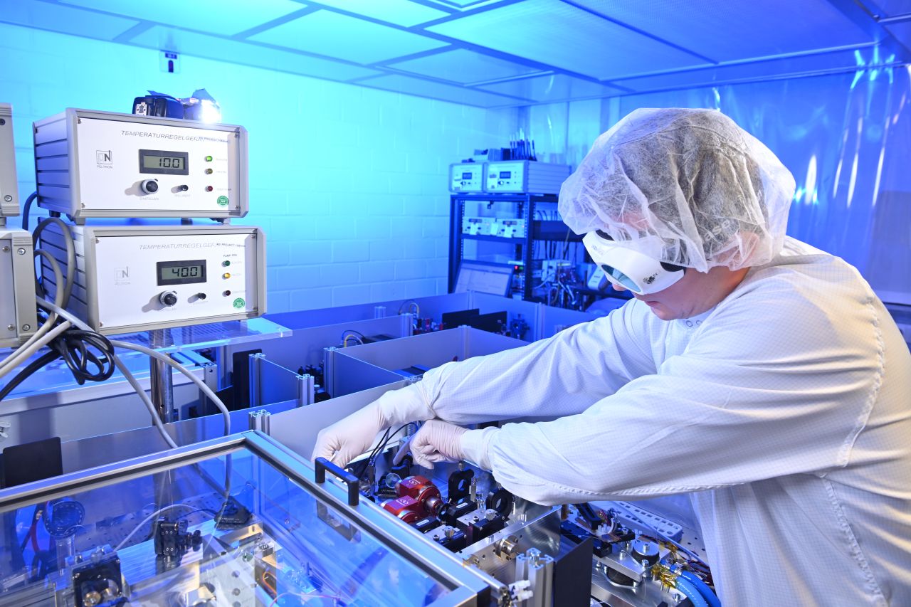
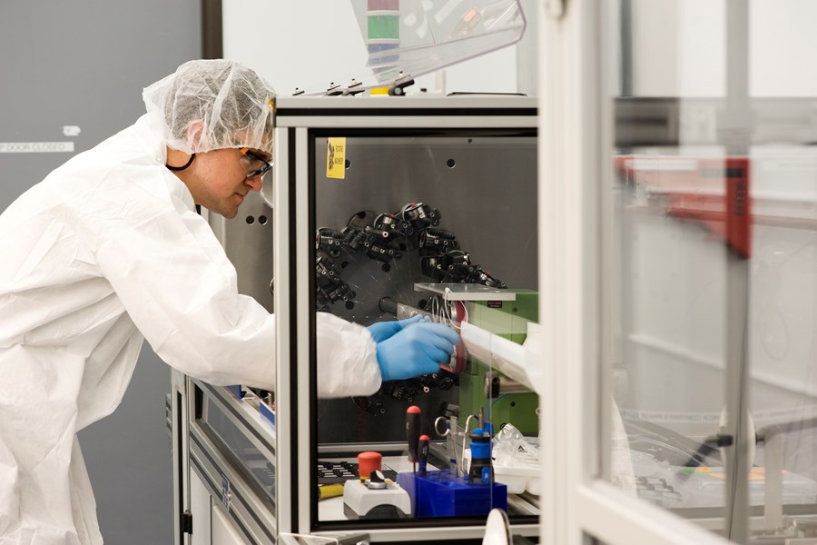
Deutschlandsberg site in Austria | TDK Electronics - TDK Europe
Capabilities - Laboratory for Atmospheric and Space Physics|LASP|CU-Boulder
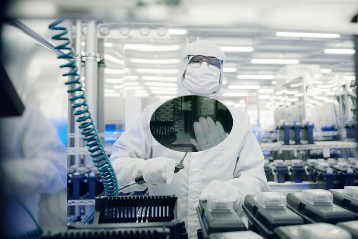
The Semiconductor Chip Manufacturing Process
Plasma patterning technique forms new optical metasurfaces ...
190+ Electric Shock Risk Caution Sign Stock Photos, Pictures & Royalty ...
College of Engineering - UC Santa Barbara | The convergence of research ...