Please enter url.
Login
Logout
Please enter url.
Isaiah Adetunmbi on LinkedIn: #100daysamplifierdesign
linkedin.com
source
Comments
Analysis, Comparison, and Experimental Validation of a Class AB Voltage
Thermal Energy Harvesting Power Supply
Low-Energy Power-ON-Reset Circuit for Dual Supply SRAM
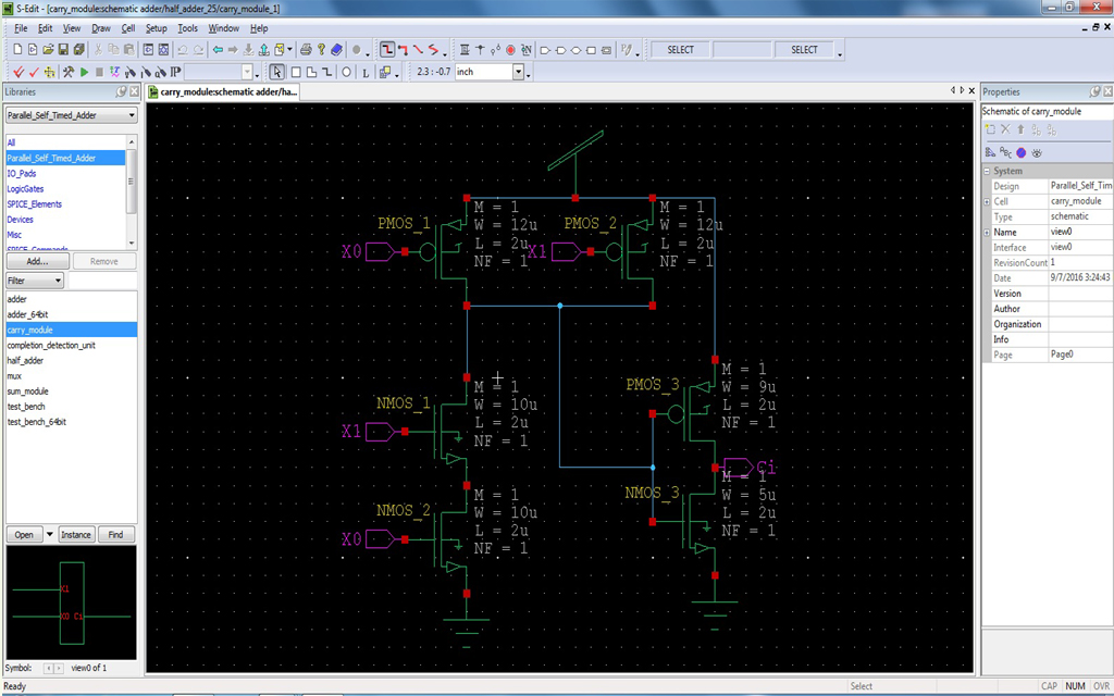
Recursive Approach to the Design of a Parallel Self Timed Adder
Fig6. PTL logic Full Adder Figure7 shows the CPL logic full adder with ...
Schematic Entry and Simulation
Power of CMOS digital Circuits in Cadence. Static, Short Circuit and ...
Lab01 EE421L Fall14
Ming Sun – Silicon achitect, design lead, researcher.
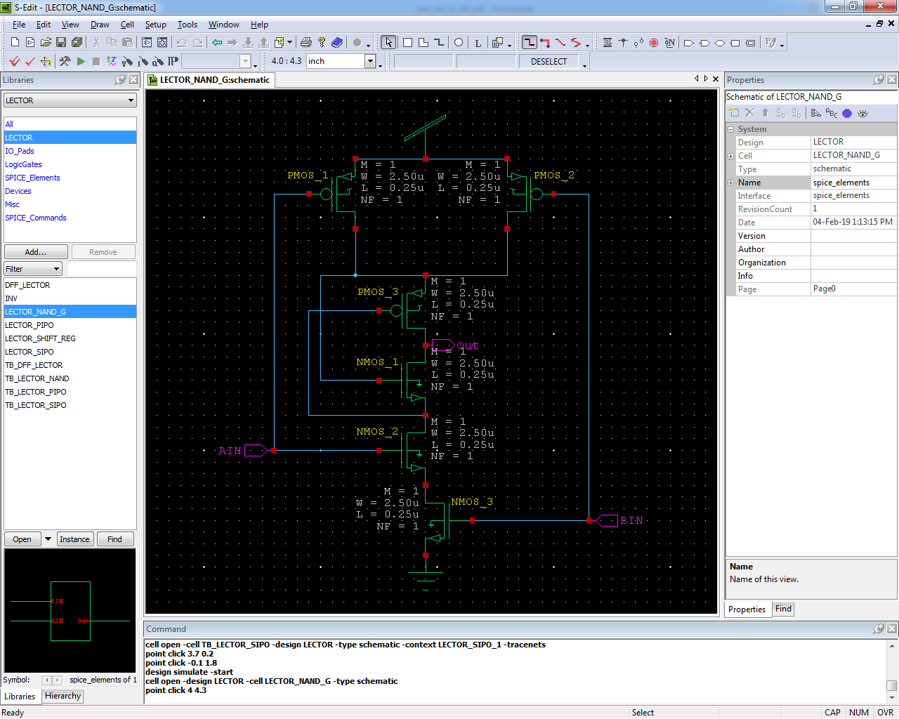
LECTOR: A Technique for Leakage Reduction in CMOS Circuits
Lab
Lab
ECE429 Lab 2 - Tutorial I: Inverter Schematic and Simulation
VLSI 4-Bit Full Adder - YouTube
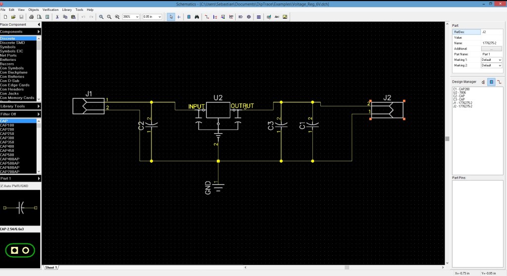
PCB Layout Design with DipTrace – An Overview | Baltic Lab
Nand gate CMOS | DSCH - YouTube
Lab
lab4
Design and Simulation of an Inverter using Tanner - YouTube
(PDF) Illustrative Comparison of MCML and CMOS Design Techniques using ...
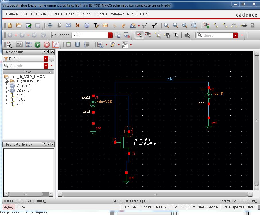
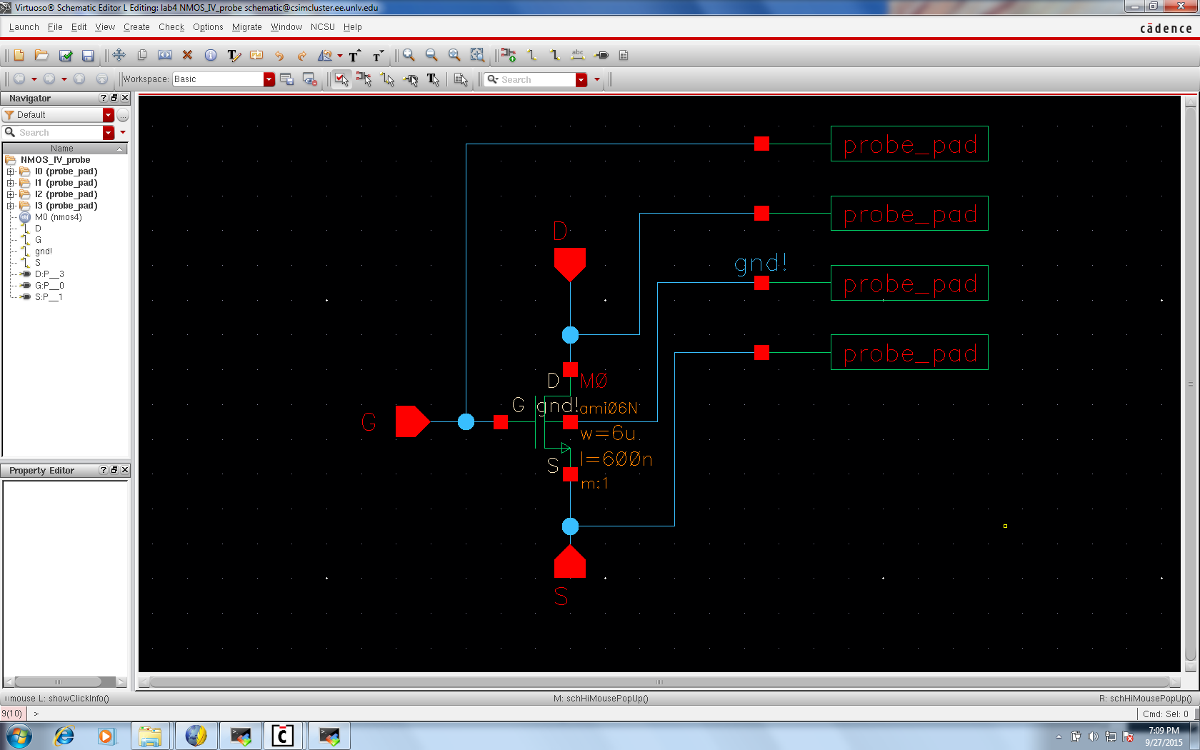
How to Save DC Operating Points’ Parameters of a MOSFET in Cadence ...
40-Gb/s 0.7-V 2:1 MUX and 1:2 DEMUX with Transformer-Coupled Technique ...
Design Methodology for Voltage Scaled Clock Distribution Networks
Schematic Generator — BAG 2.0 documentation
GitHub - shashwat0426/MOSFET: MOSFET(NMOS & PMOS) based different logic ...
Fixing xschem on Mac using install_name_tool (M1 running Big Sur) - YouTube
Lab_01
Soft-Error-Aware Read-Stability-Enhanced Low-Power 12T SRAM
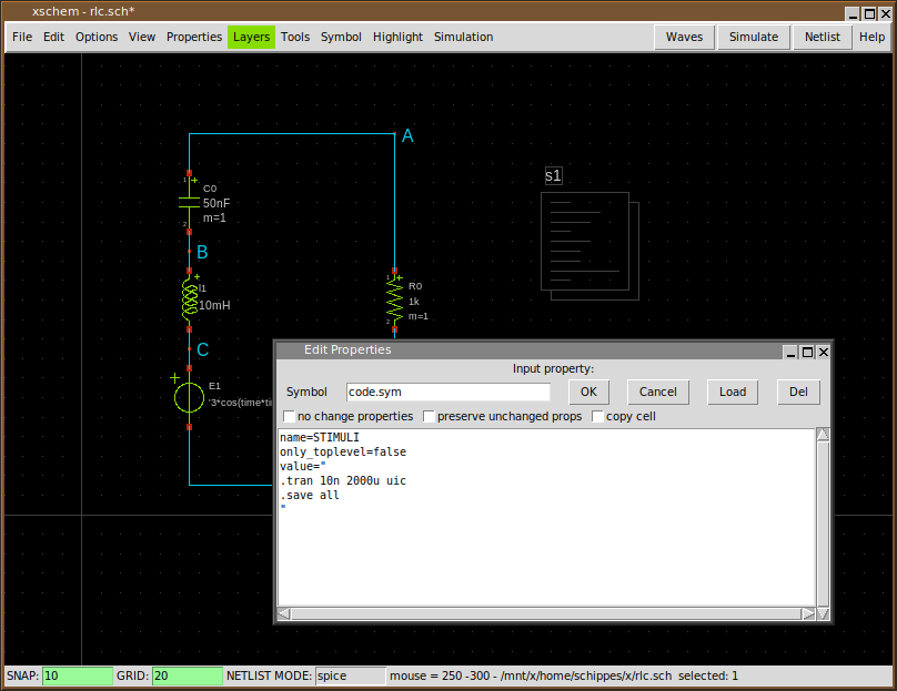
XSCHEM TUTORIAL
Lab
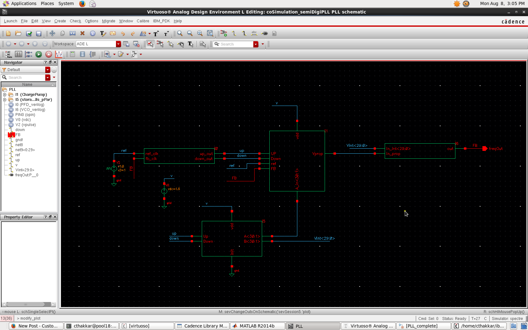
Problem with Co-simulation: Cadence Virtuoso and Matlab - Custom IC ...
ECE468 Cadence Virtuoso tutorial - - YouTube
[PDF] DESIGN OF RADIX-4 BOOTH MULTIPLIER USING MGDI AND P TL TECHNIQUES ...
About Buffer Sizing
DxDesigner | Compatibility Database | CodeWeavers


![[PDF] DESIGN OF RADIX-4 BOOTH MULTIPLIER USING MGDI AND P TL TECHNIQUES ...](https://d3i71xaburhd42.cloudfront.net/e0e6ac616120244fbfbd3933e5756f1b8182d55f/4-Figure4-1.png)