


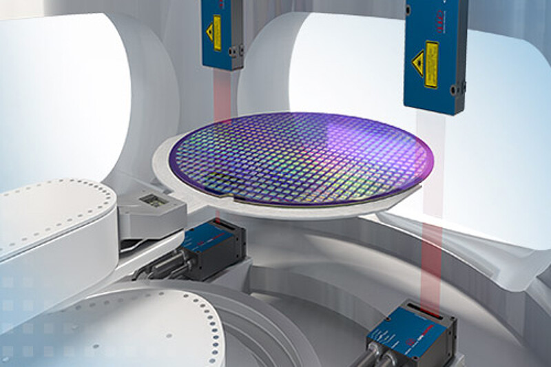


Support discovery through extensive collections of scientifically-accurate wafer eccentricity deviation measurement method based on line-scanning photographs. accurately representing photography, images, and pictures. designed to support academic and research goals. Our wafer eccentricity deviation measurement method based on line-scanning collection features high-quality images with excellent detail and clarity. Suitable for various applications including web design, social media, personal projects, and digital content creation All wafer eccentricity deviation measurement method based on line-scanning images are available in high resolution with professional-grade quality, optimized for both digital and print applications, and include comprehensive metadata for easy organization and usage. Explore the versatility of our wafer eccentricity deviation measurement method based on line-scanning collection for various creative and professional projects. Reliable customer support ensures smooth experience throughout the wafer eccentricity deviation measurement method based on line-scanning selection process. Time-saving browsing features help users locate ideal wafer eccentricity deviation measurement method based on line-scanning images quickly. Whether for commercial projects or personal use, our wafer eccentricity deviation measurement method based on line-scanning collection delivers consistent excellence. Multiple resolution options ensure optimal performance across different platforms and applications. Our wafer eccentricity deviation measurement method based on line-scanning database continuously expands with fresh, relevant content from skilled photographers.