Please enter url.
Login
Logout
Please enter url.
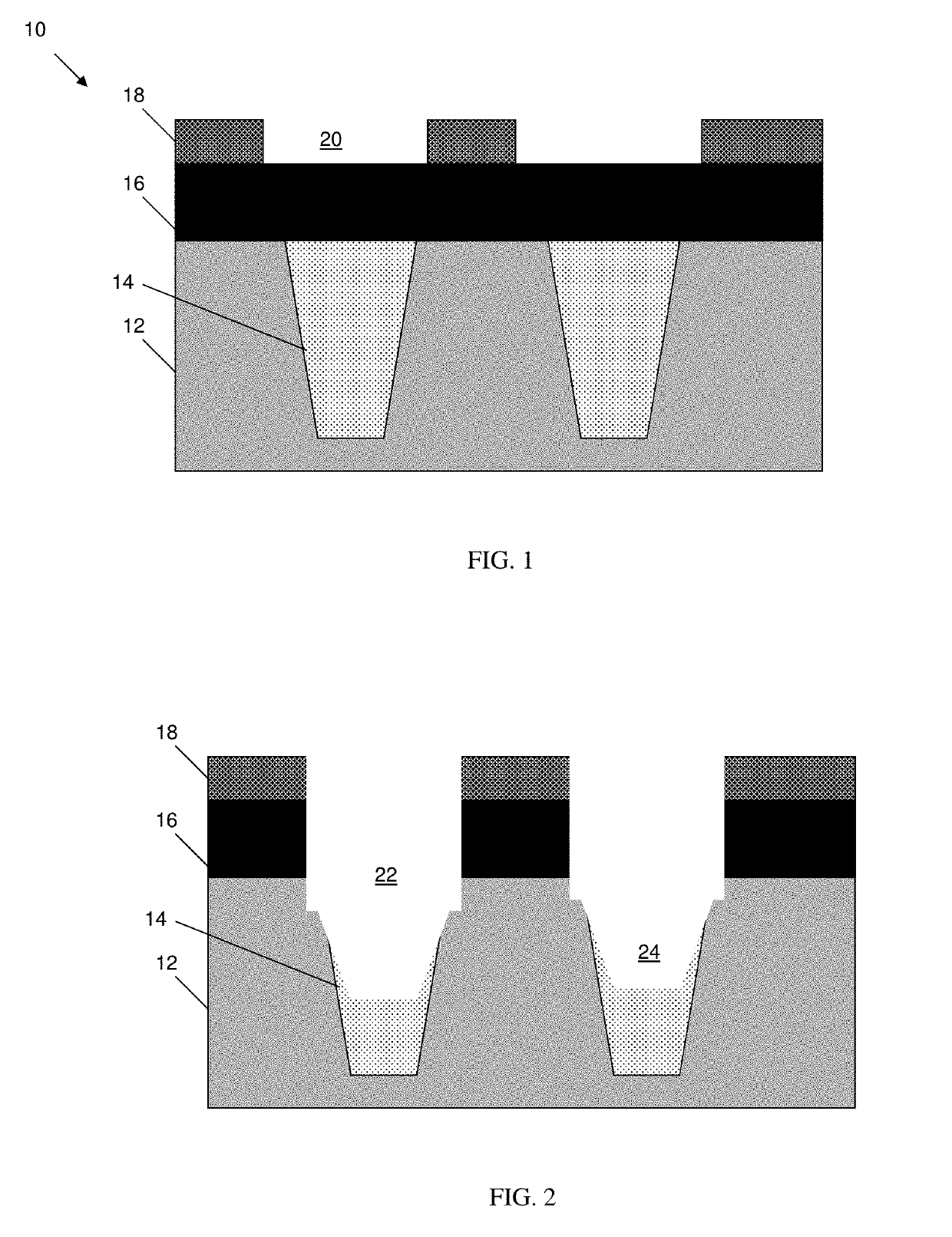
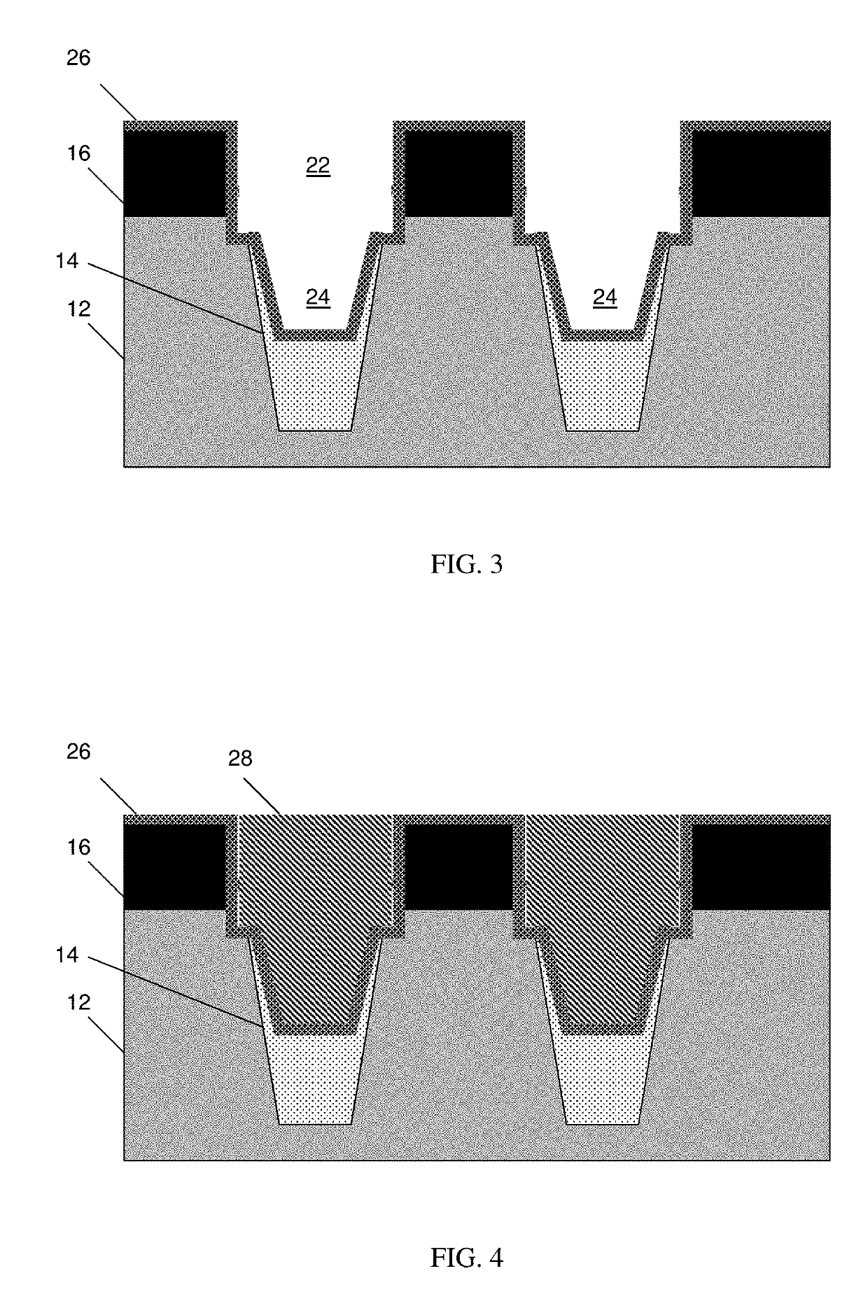
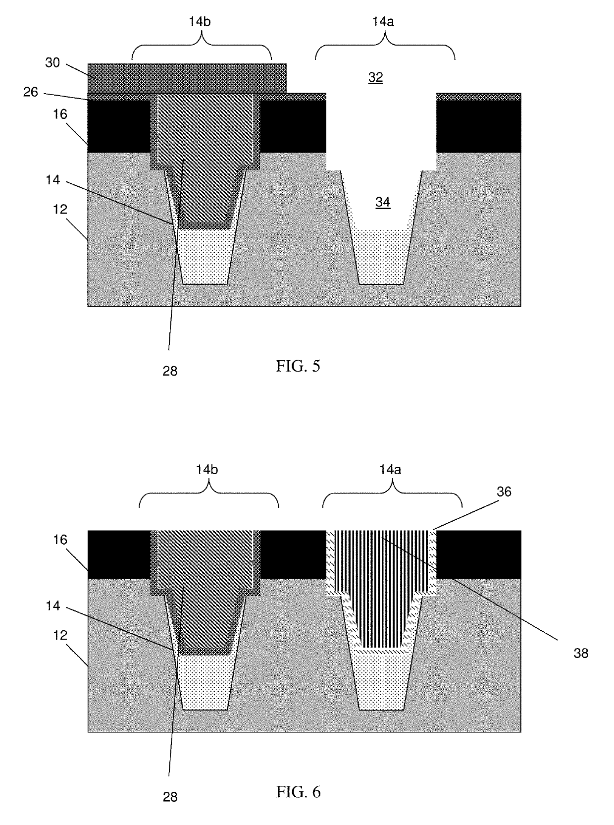
Selective shallow trench isolation (STI) fill for stress engineering in ...
eureka.patsnap.com
source
Comments
Selective shallow trench isolation (STI) fill for stress engineering in ...
Selective shallow trench isolation (STI) fill for stress engineering in ...
The steps involved in stamp lithography. (a) Preparation of base PDMS ...
Method of forming semiconductor material in trenches having different ...
Patent US6713365 - Methods for filling shallow trench isolations having ...
Schematic showing the gas-assisted hot embossing facility and process ...
Flash memory structure, memory array and fabrication method thereof ...
Figure 10 from A new C-MOS technology using anisotropic etching of ...
Figure 1 from Latch-back-free self-aligned power MOSFET structure with ...
Structures with thinned dielectric material Patent Grant Bao , et al ...
Structure and its formation stages (a), (b), (c), (d) of 3D thin film ...
Fabrication process of the nanocomposite based spatial light modulator ...
Overturned thin film device with self-aligned gate and source/drain (S ...
Microprobe fabrication process. (a) Electroplating Cu sacrificial ...
Micro-electro-mechanical system (MEMS) and related actuator bumps ...
Patent US20050151222 - Shallow trench isolation process and structure ...
Brevet US6187651 - Methods of forming trench isolation regions using ...
Figure 1 from Low-temperature processed polycrystalline silicon thin ...
Sequence used in the microfabrication on the silicon surface ...
The main stages of technological flow. | Download Scientific Diagram
Cross-sectional view of the major fabrication process steps for the ...
Cross-section of the post process steps in the fabrication process. (a ...
The emitter-up SiGe-HBT structure used in the simulations. | Download ...
Semiconductor fin length variability control Patent Grant Joseph , et ...
Schematic diagram of the transmission line in the DEOS system ...
Schematic of fabrication process started by (a) deposition of SiO2 and ...
Washing liquid for semiconductor substrate and method of producing ...
Schematic structure of the extended gate ISFET. | Download Scientific ...
Self-aligned silicide/germanide formation to reduce external resistance ...
Dummy gate isolation and method of production thereof Patent Grant ...
(a)-(i) RFP technology flow. For clarity, only one cell is shown. (j ...
Patent US8299533 - Vertical NPNP structure in a triple well CMOS ...
photoresist as the etching mask. The etch rate is of about 40 nm s -1 ...
Method for manufacturing color film substrate and color film substrate ...
Schematic process flow for the fabrication of the piezoelectric SiC ...