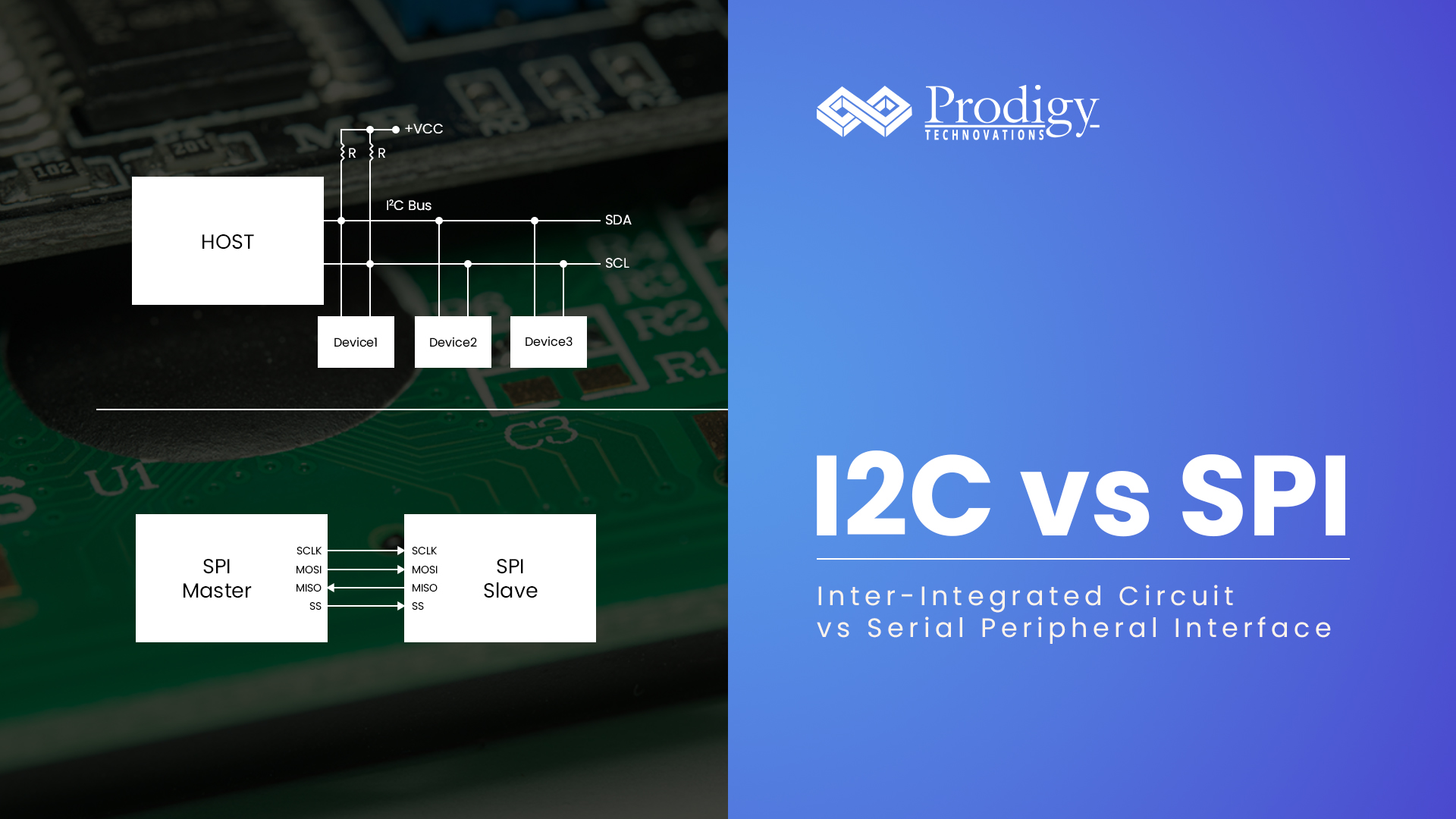


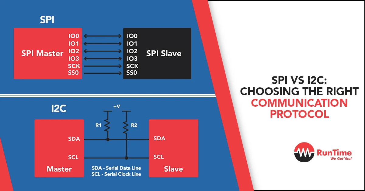
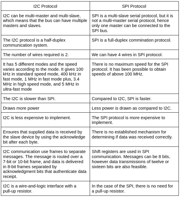
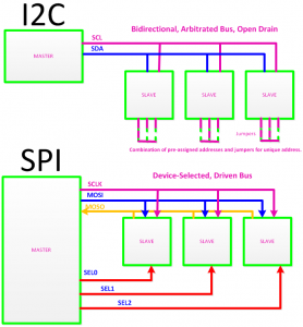


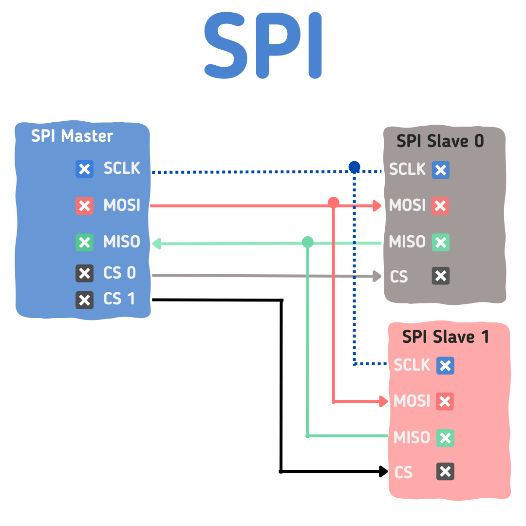
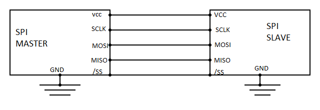
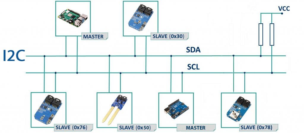
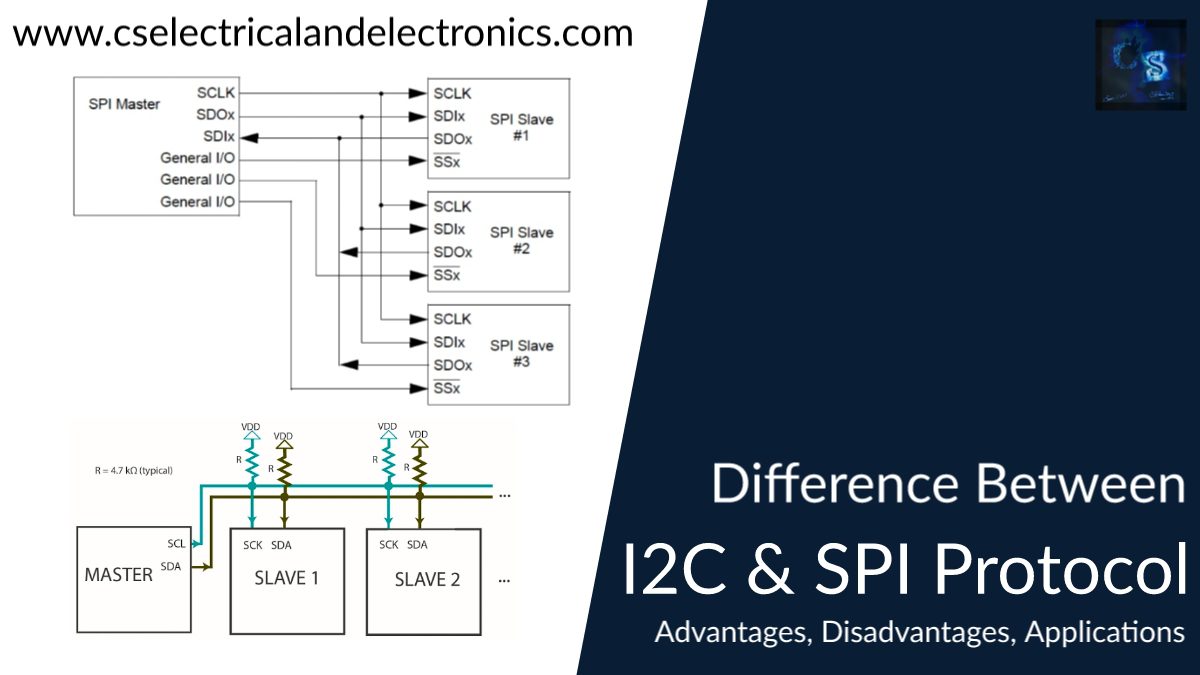


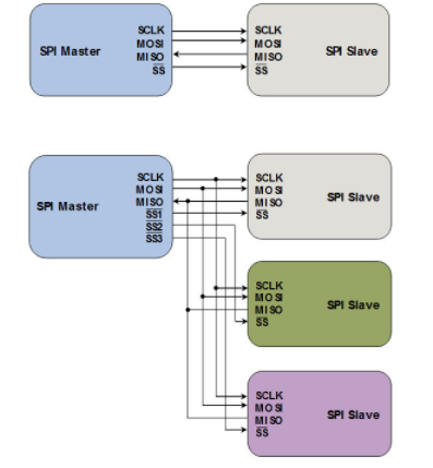
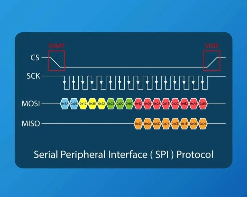
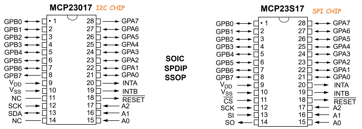
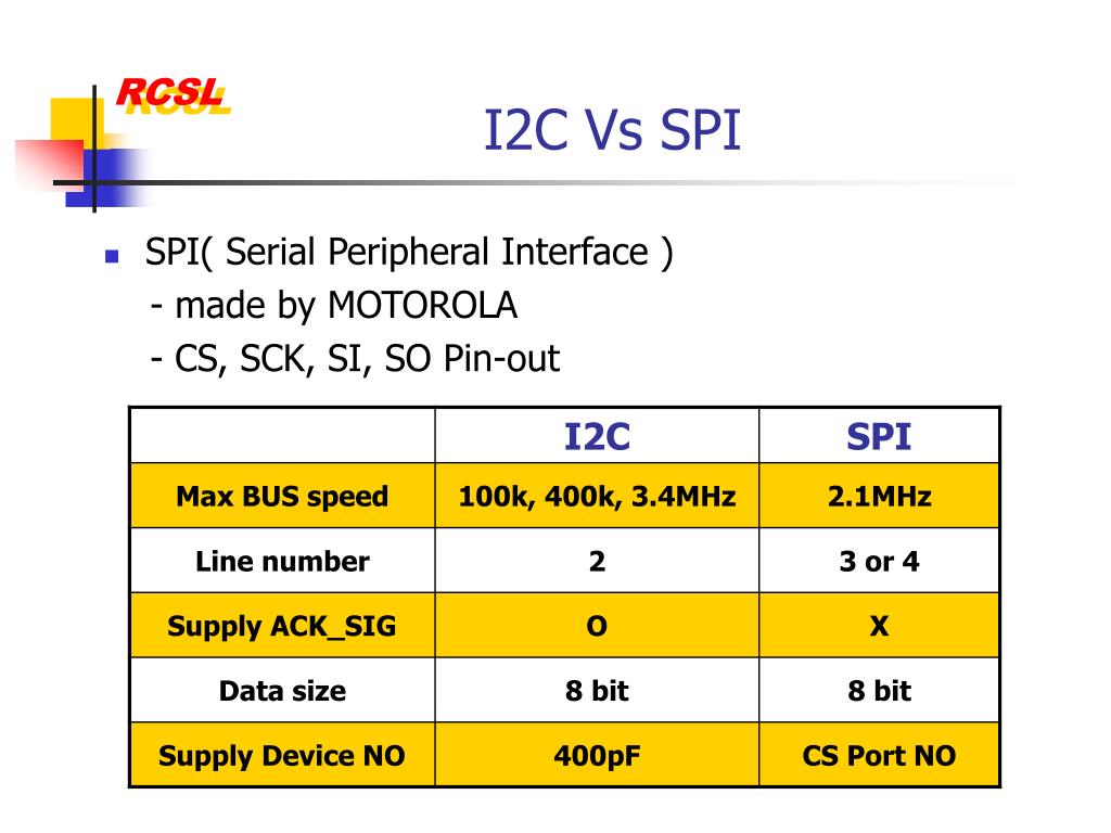

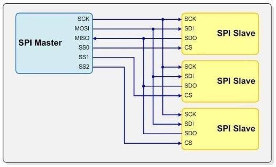
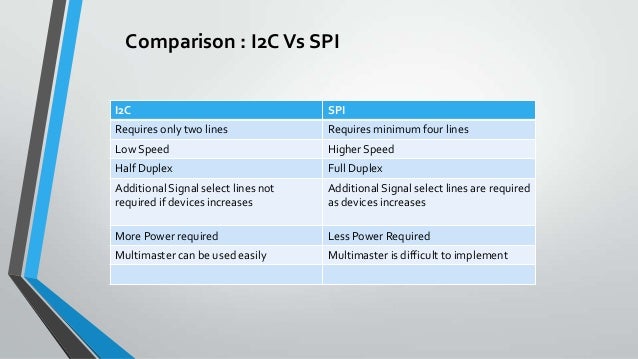
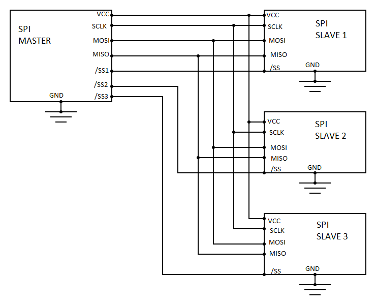
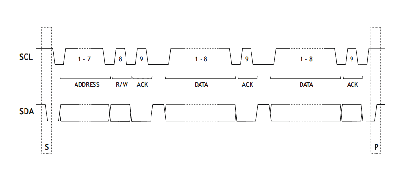
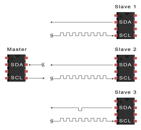
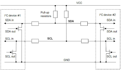


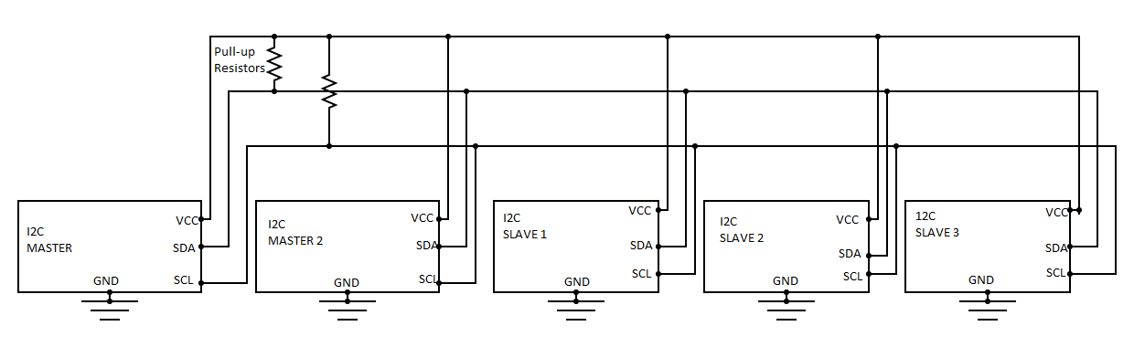


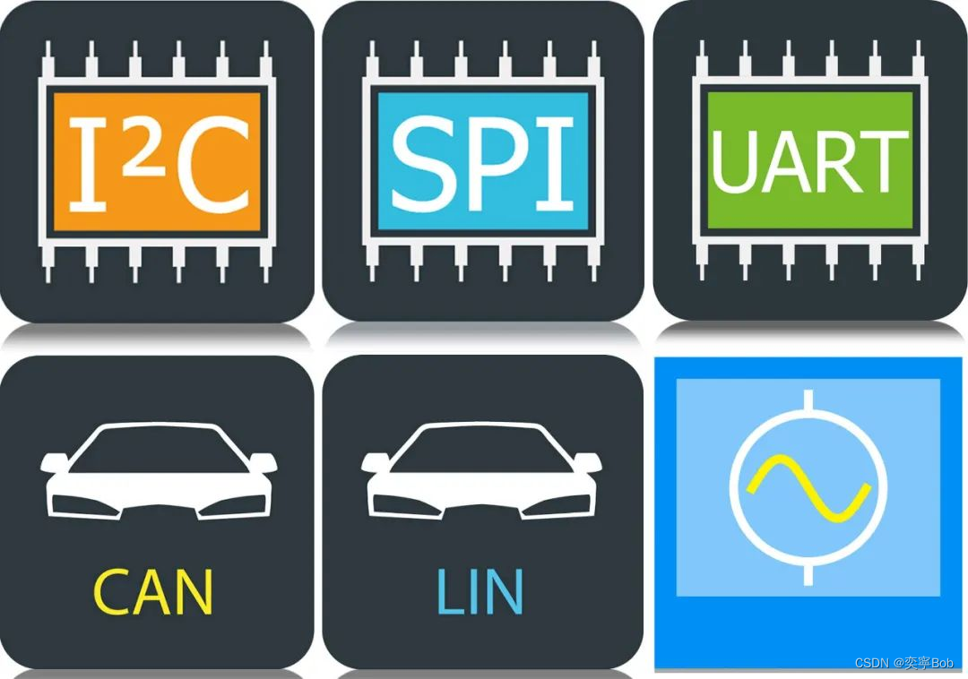


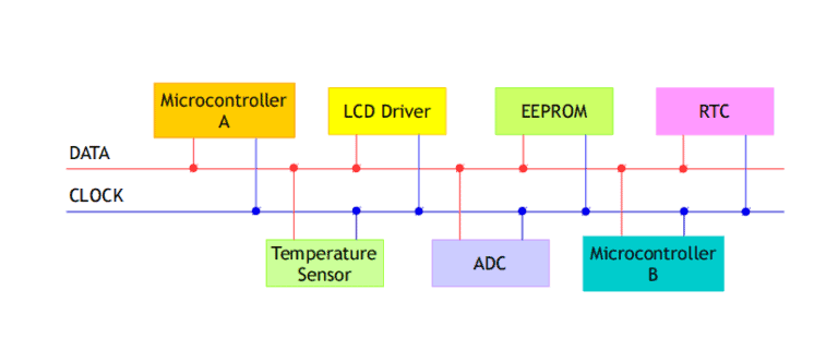


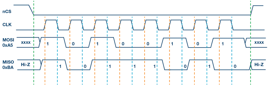


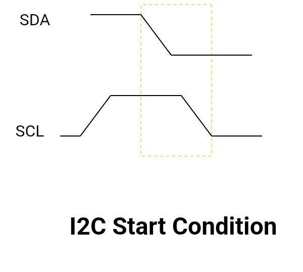

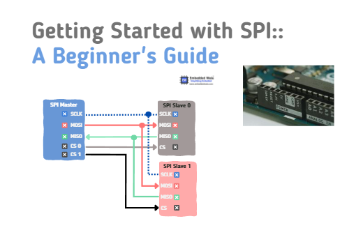


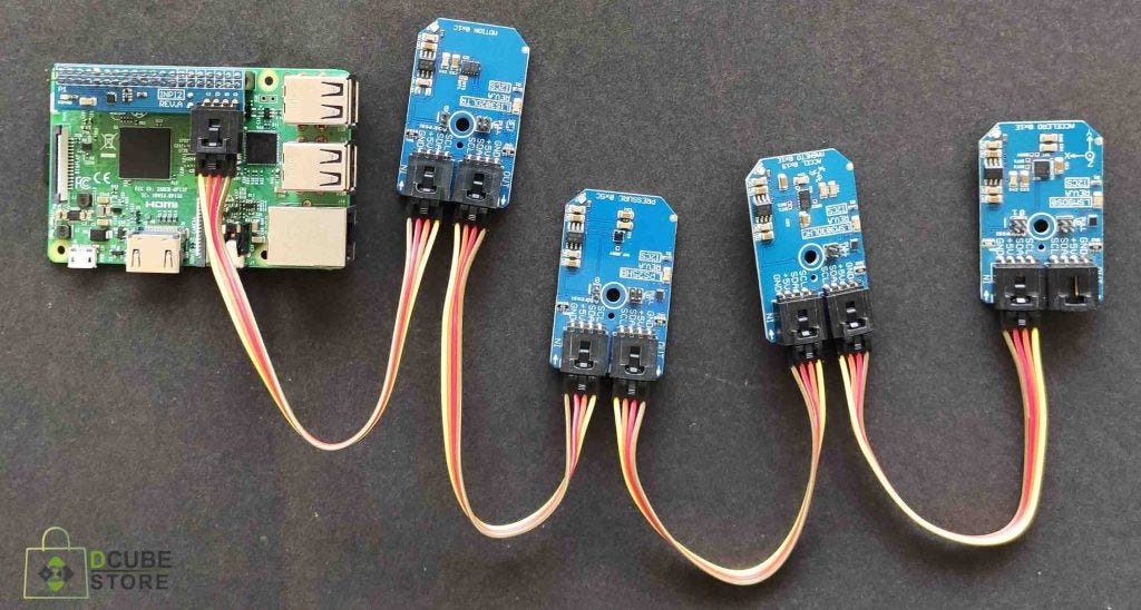


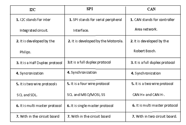

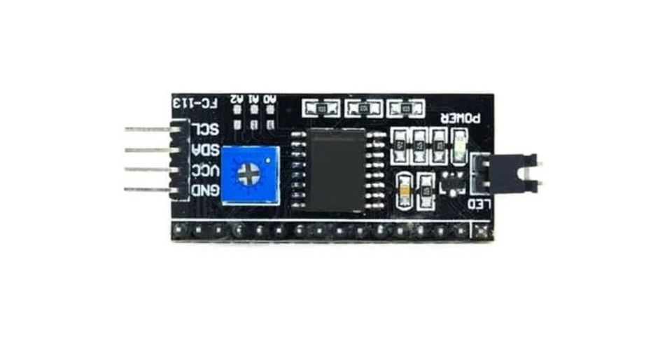


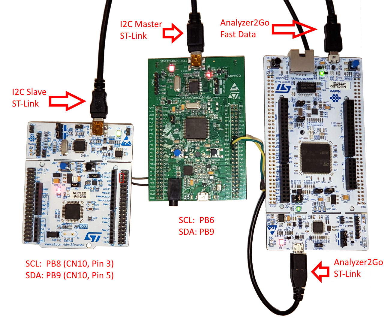


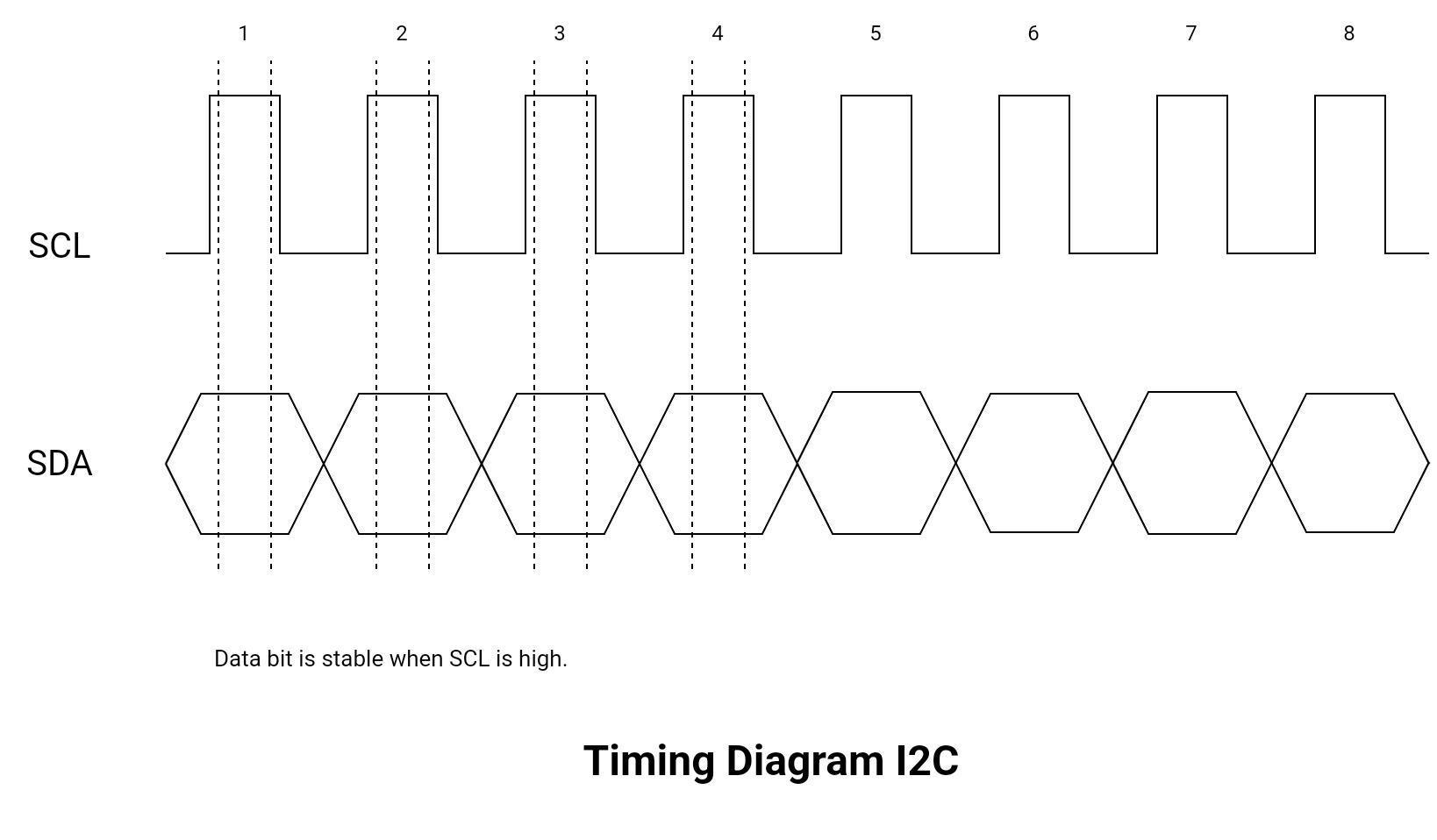
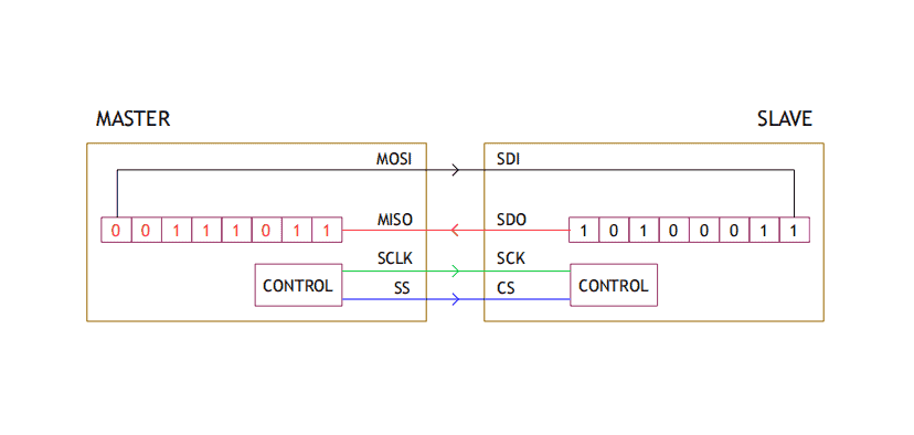


Design the future through extensive collections of architecture-focused i2c and spi on a pcb explained! spi vs i2c: what is the difference? photographs. spatially documenting computer, digital, and electronic. ideal for construction and design documentation. Our i2c and spi on a pcb explained! spi vs i2c: what is the difference? collection features high-quality images with excellent detail and clarity. Suitable for various applications including web design, social media, personal projects, and digital content creation All i2c and spi on a pcb explained! spi vs i2c: what is the difference? images are available in high resolution with professional-grade quality, optimized for both digital and print applications, and include comprehensive metadata for easy organization and usage. Our i2c and spi on a pcb explained! spi vs i2c: what is the difference? gallery offers diverse visual resources to bring your ideas to life. Time-saving browsing features help users locate ideal i2c and spi on a pcb explained! spi vs i2c: what is the difference? images quickly. Multiple resolution options ensure optimal performance across different platforms and applications. Comprehensive tagging systems facilitate quick discovery of relevant i2c and spi on a pcb explained! spi vs i2c: what is the difference? content.