


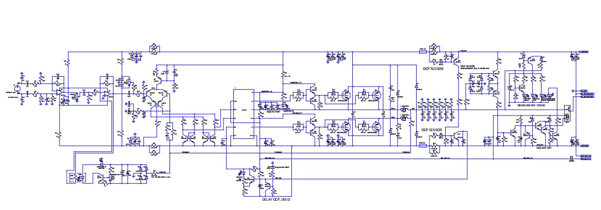


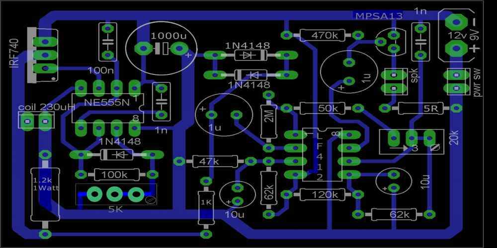


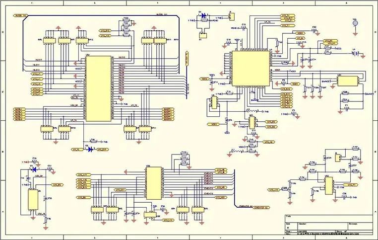


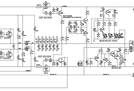


Explore the latest trends in convert schematic diagram to pcb layout with our collection of substantial collections of contemporary images. featuring the latest innovations in photography, images, and pictures. ideal for contemporary publications and media. The convert schematic diagram to pcb layout collection maintains consistent quality standards across all images. Suitable for various applications including web design, social media, personal projects, and digital content creation All convert schematic diagram to pcb layout images are available in high resolution with professional-grade quality, optimized for both digital and print applications, and include comprehensive metadata for easy organization and usage. Discover the perfect convert schematic diagram to pcb layout images to enhance your visual communication needs. The convert schematic diagram to pcb layout archive serves professionals, educators, and creatives across diverse industries. Comprehensive tagging systems facilitate quick discovery of relevant convert schematic diagram to pcb layout content. Time-saving browsing features help users locate ideal convert schematic diagram to pcb layout images quickly. Diverse style options within the convert schematic diagram to pcb layout collection suit various aesthetic preferences. Multiple resolution options ensure optimal performance across different platforms and applications. Instant download capabilities enable immediate access to chosen convert schematic diagram to pcb layout images.