Please enter url.
Login
Logout
Please enter url.
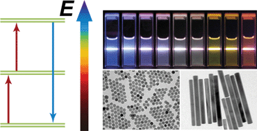
Schematic illustration of the self-frequency conversion NW laser and ...
researchgate.net
source
Comments
Schematic illustration of the self-frequency conversion NW laser and ...
Bioinspired microfluidic system design and microfabrication. a ...
(A) Controlling the plasmonic resonance of graphene by changing the ...
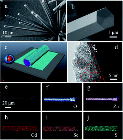
Facile synthesis and optical properties of colloidal quantum dots/ZnO ...
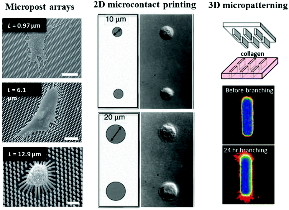
New advances in probing cell–extracellular matrix interactions ...
Composition and atom structure of CVD-grown Sb 2 Se 3 NWs. a ...
Device for demonstrating anisotropic flow tilt in the parallelogram ...
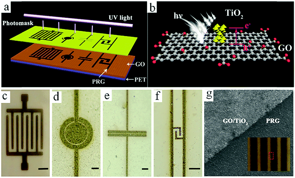
Processing and manufacturing of graphene-based microsupercapacitors ...
Polyberg Develops and Scales up Silver Nanowire (Agnw) – FCAD Group
(a−d) Nucleation optimization of InP NWs on a (001) substrate where the ...
(a and c) TEM images of ZnO@In 2 O 3 heterojunction nanowires, (b ...
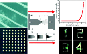
a) Schematic representation of the two-beam DLIP approach on flat ...
Surface-guided epitaxial CsPbBr3 nanowires on C-plane sapphire (a) An ...
Inorganic semiconductor nanostructures and their field-emission ...
Holography, Fourier Optics, and Beyond Photonic Crystals: Holographic ...
(a) HRTEM image of GNR-HA powders synthesized via solvothermal process ...
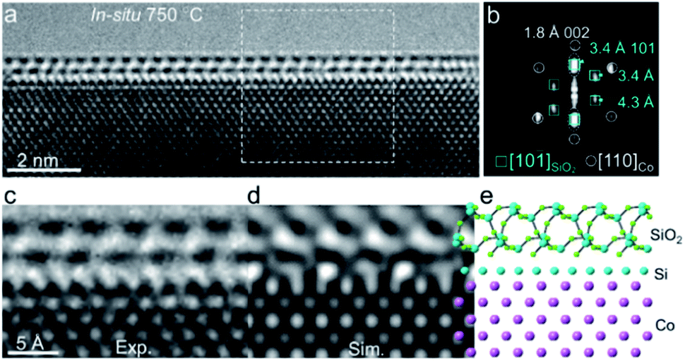
Atomic origins of the strong metal–support interaction in silica ...
Synthetic methods for perovskite nanocrystal superlattices. a ...
Recent advances in the chemistry of lanthanide-doped upconversion ...
SEM images, (b) schematic diagram, (c) image of the BNS device ...
Anisotropic quasi-one-dimensional layered transition-metal ...
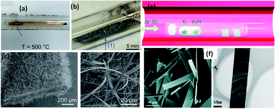
a Scanning electron microscopy image of the nanowires where the ...
Ultrafast laser inscription. Left shows an illustration of the ...
ABF-STEM images of water-soaked (a) NaNM and (b) NaNCMT. HAADF-STEM ...
(a) BF image of a GaAs nanowire grown under conditions where 100% ...
(a) TEM images of MAPbI3 nanowires with atomic resolution. Adapted with ...
Inhibited/enhanced fluorescence of embedded fluorescent defects by ...
Applied Sciences | Free Full-Text | Optical Beamforming Networks for ...
a) FESEM and b–e) the corresponding elemental‐mapping images (Mo, Ga ...
(a) A plan-view STEM image; (b) HADDF cross section image; (c) EDS ...
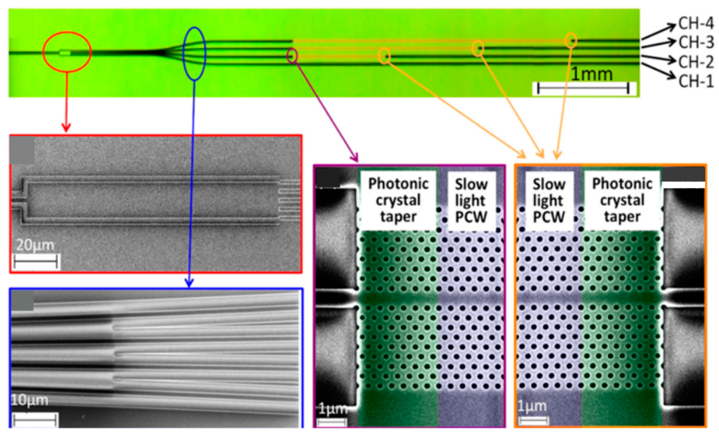
(a) Left: Scanning electron microscope (SEM) images of a fabricated ...
Templated nanoscale porous carbons - Nanoscale (RSC Publishing) DOI:10. ...
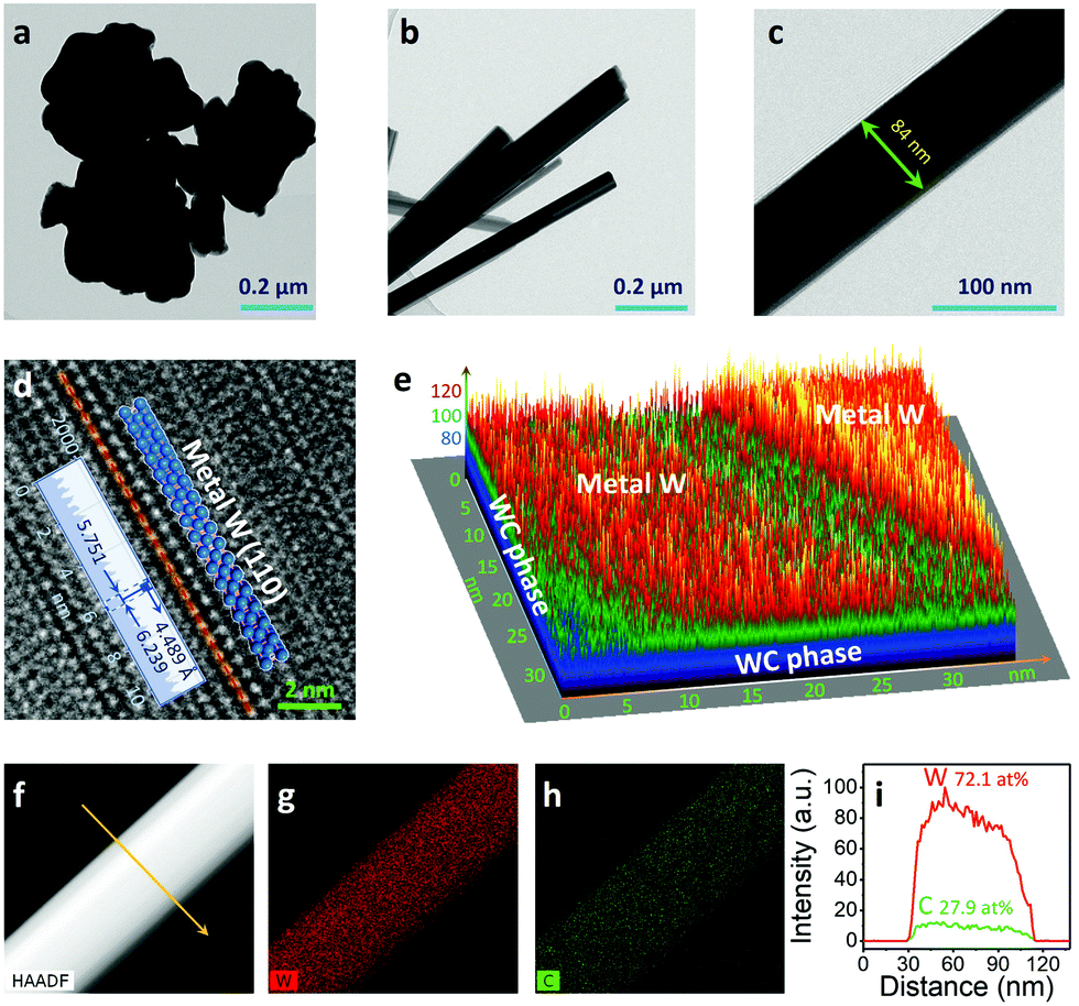
Realizing the extraction of carbon from WC for in situ formation of W ...
Color from hierarchy: Diverse optical properties of micron-sized ...
(a) Schematic model and (b) its typical TEM image of an incompletely ...