Please enter url.
Login
Logout
Please enter url.
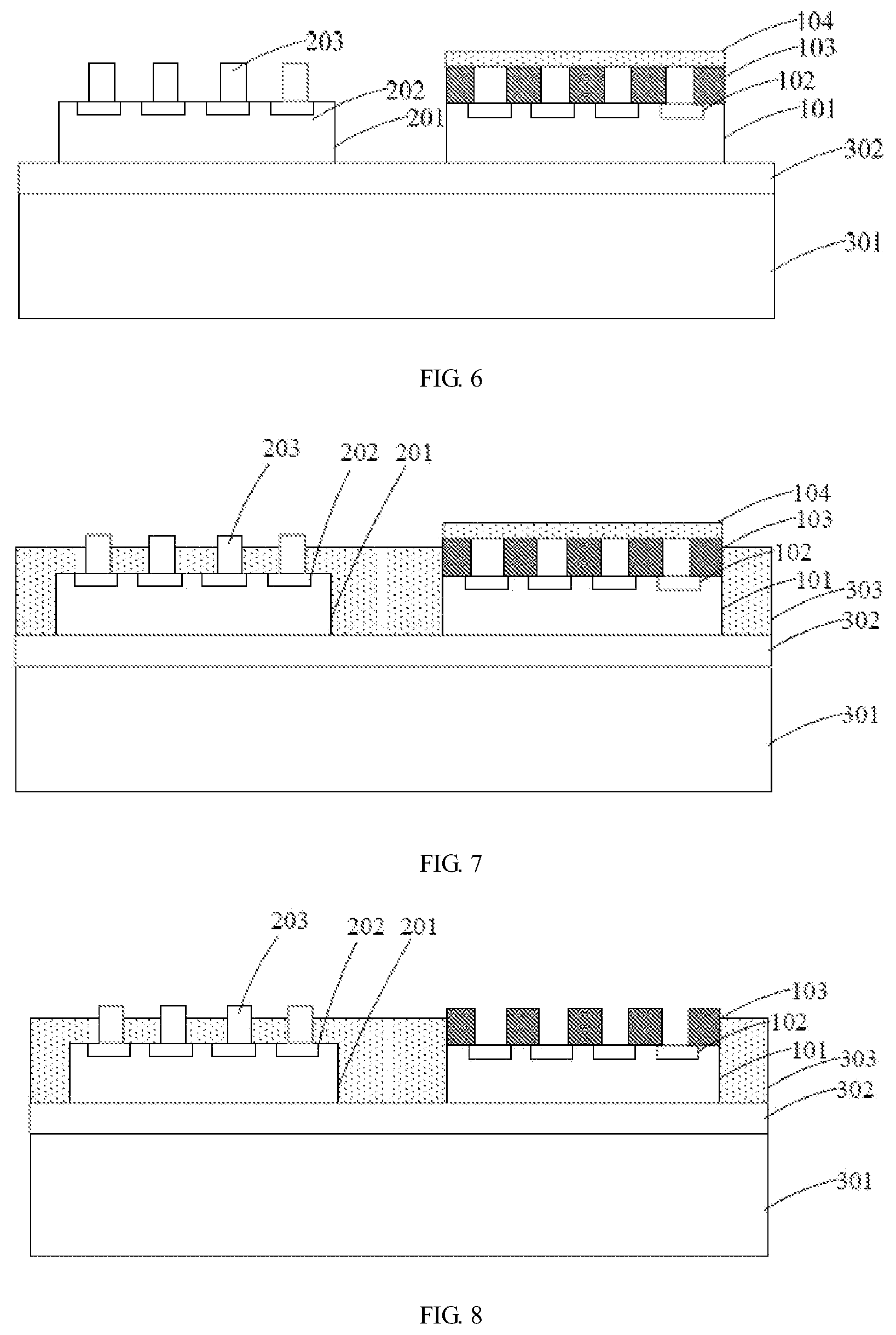
Package method and package structure of fan-out chip Patent Grant Qiu ...
uspto.report
source
Comments
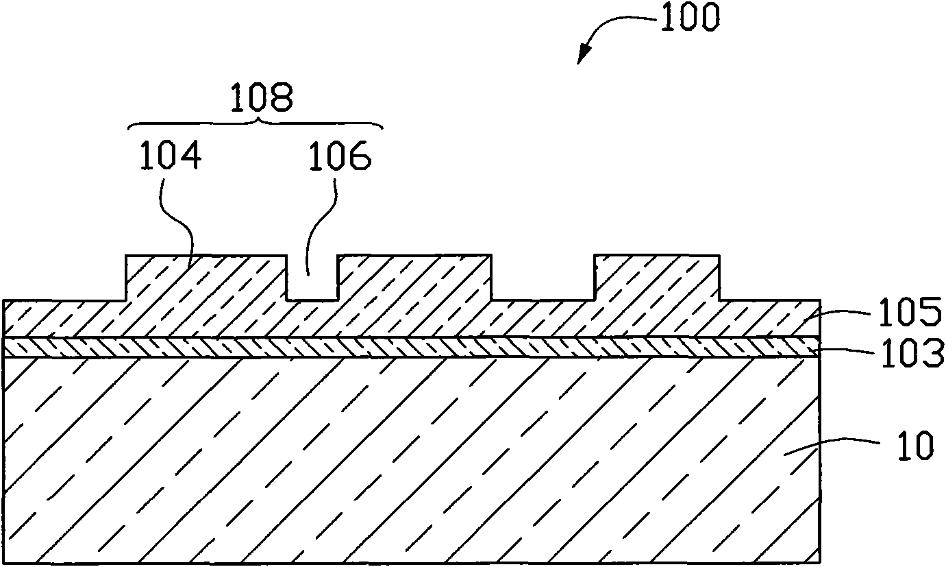
Process of forming semiconductor apparatus mounting on substrate Patent ...
Assay Plates, Reader Systems And Methods For Luminescence Test ...
Packaging Method And Packaging Structure For Semiconductor Chip Wang ...
Patent US7713834 - Method of forming isolation regions for integrated ...
Methods and apparatuses to form self-aligned caps Patent Grant Boyanov ...
Mold for nano-imprinting and method of manufacturing the same - Eureka ...
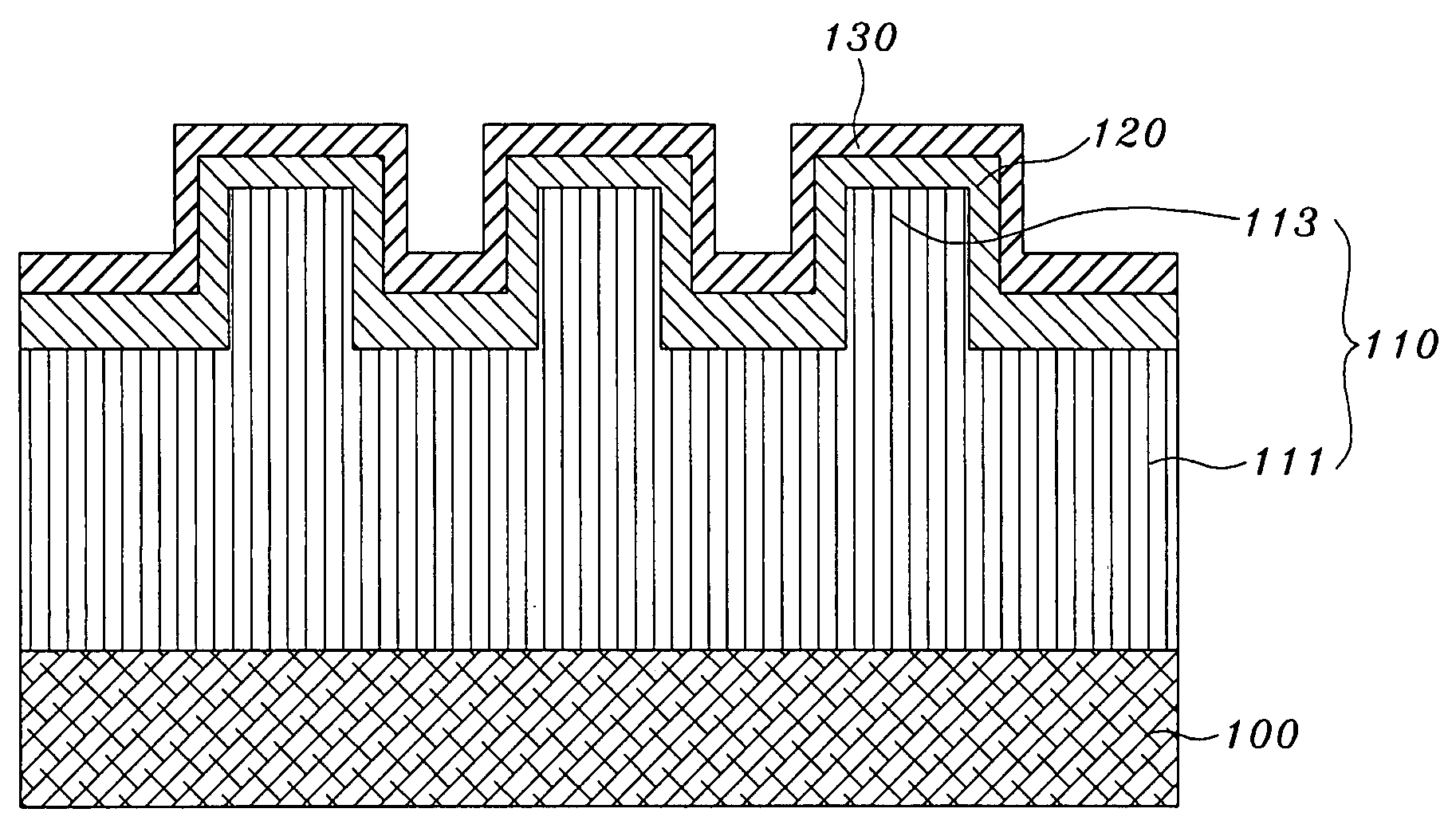
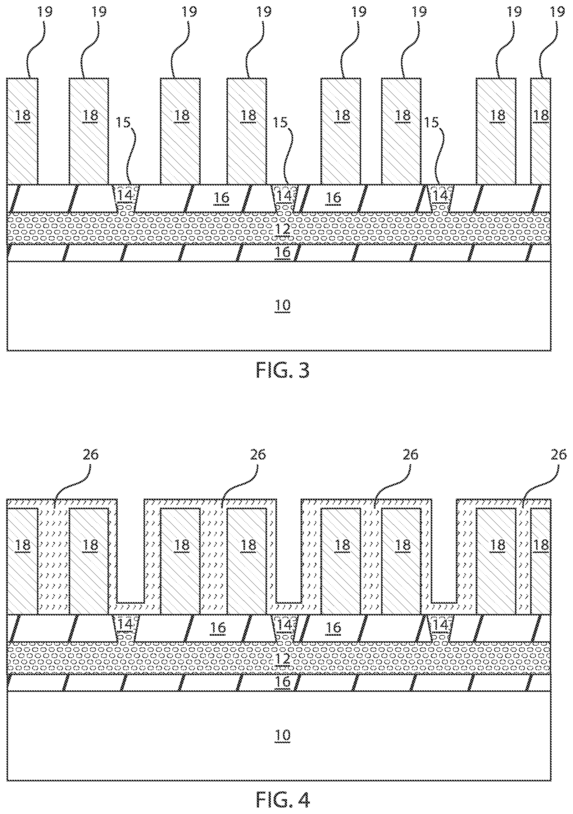
SEMICONDUCTOR DEVICE WITH FINE METAL LINES FOR BEOL STRUCTURE AND ...
Heater to control bubble and inkjet printhead having the heater ...
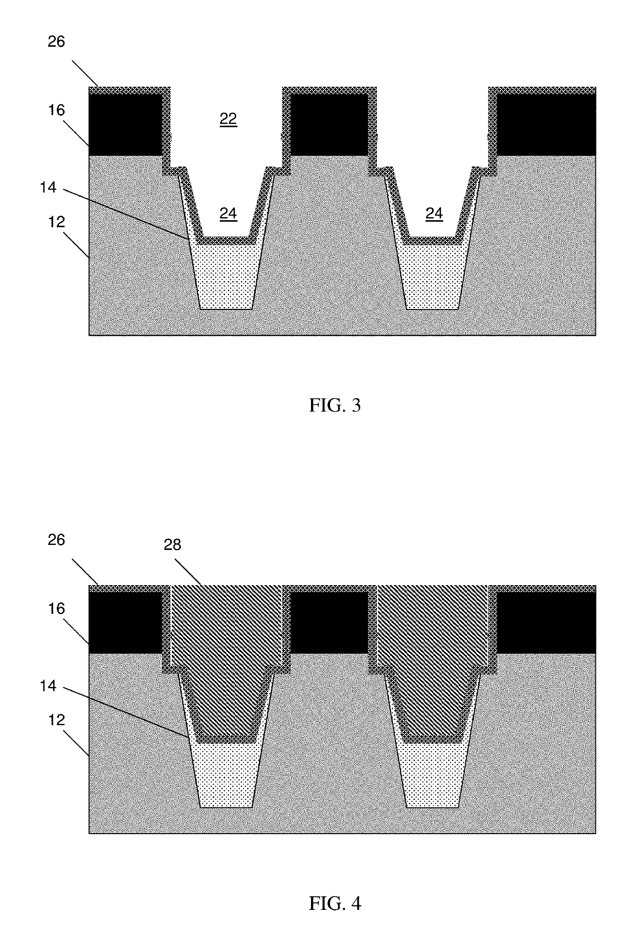
Patent US6713365 - Methods for filling shallow trench isolations having ...
Thermal-sprayed bonding of a ceramic structure to a substrate Patent ...
Nano-imprint template and preparation method thereof - Eureka | Patsnap
Patent US7071096 - Method of forming a conductive barrier layer within ...
Selective shallow trench isolation (STI) fill for stress engineering in ...
Rram Cells In Crossbar Array Architecture Kong; Dexin ; et al ...
Flash memory structure, memory array and fabrication method thereof ...
Capacitive touch sensor - Eureka | Patsnap
Semiconductor sensor device and semiconductor sensor device ...
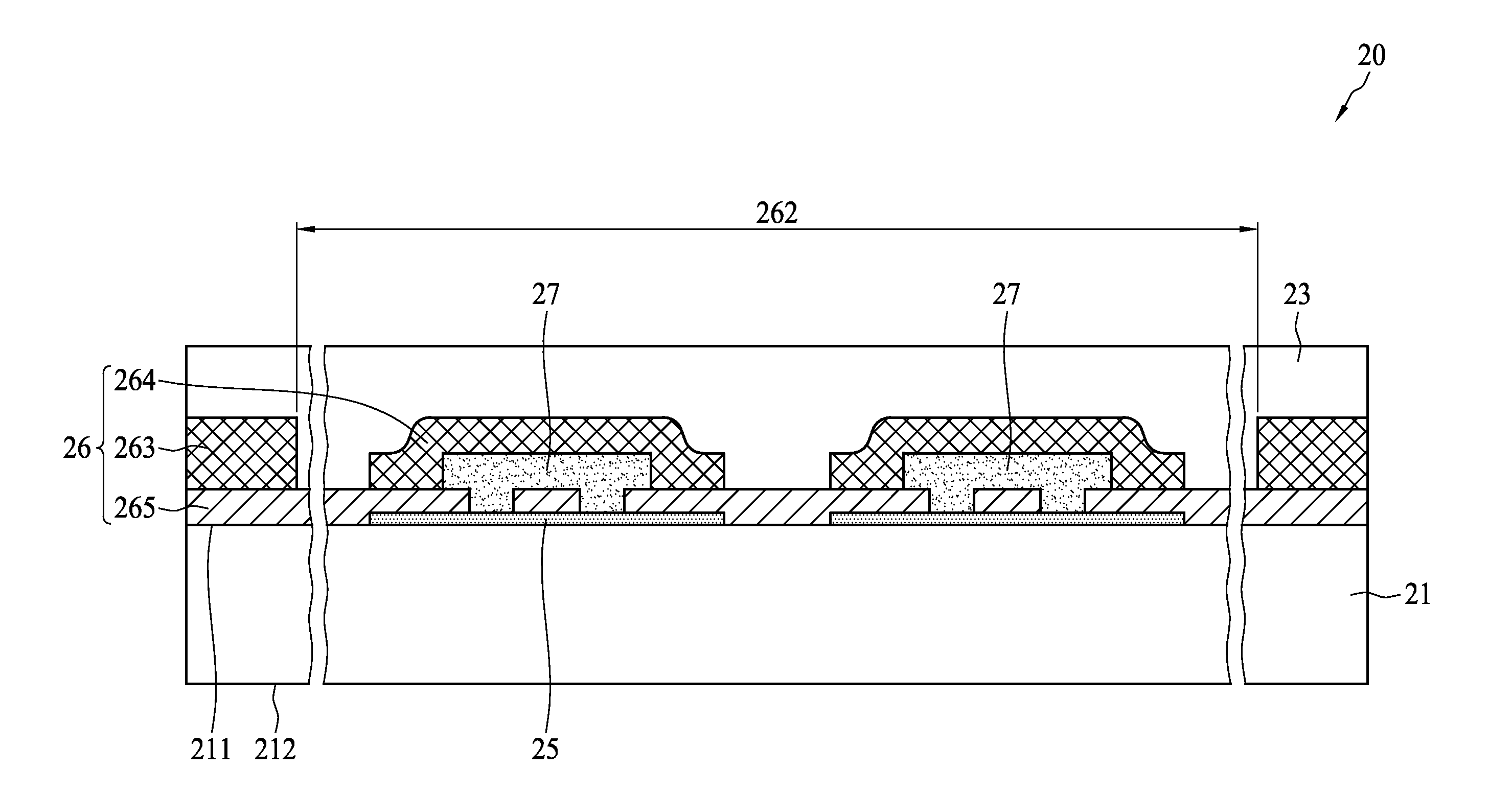
Semiconductor Device USAMI; Tatsuya ; et al. [RENESAS ELECTRONICS ...
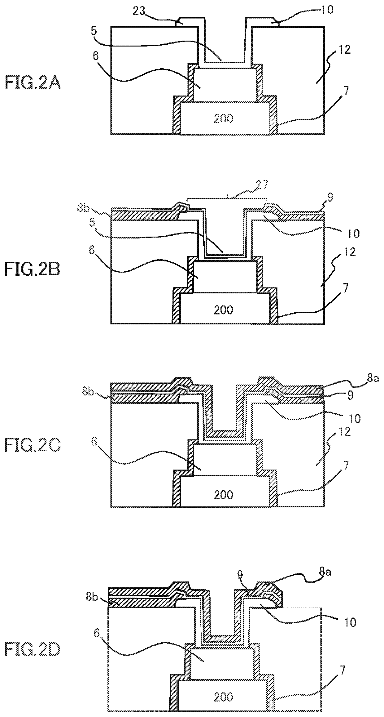
Manufacturing Method Of Array Substrate And Array Substrate LV; Xiaowen ...
Smoothing Surface Roughness Of Iii-v Semiconductor Fins Formed From ...
Fringe field switching mode transflective liquid crystal display ...
Chip-scale package - Eureka | Patsnap
Electromigration resistant and profile consistent contact arrays Patent ...
Patent US7755184 - Liquid metal thermal interface material system ...
Fabrication method of electronic module Patent Grant Chen , et al. Oc ...
SEMICONDUCTOR DEVICE WITH FINE METAL LINES FOR BEOL STRUCTURE AND ...
Semiconductor Device And Method For Manufacturing The Semiconductor ...
Increased isolation of diffusion breaks in FinFET devices using an ...
Ultrasonic fingerprint sensor package, ultrasonic fingerprint ...
Oxide semiconductor TFT array substrate and method for forming the same ...
Carbonics, Inc. executes license of carbon IP bucket – Carbonics Inc.
Method For Polishing Substrate Including Functional Chip TOGAWA ...
PHOTOMASK BLANK - Patent 3373067
Thin-film transistor, method of fabricating thin-film transistor, and ...
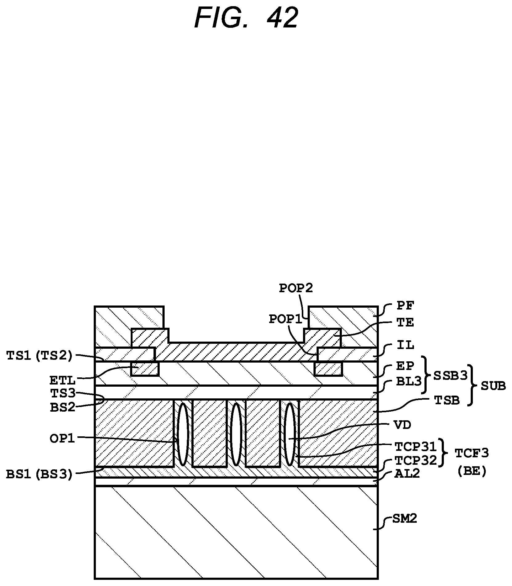
Three-dimensional die-stacking package structure and method for ...