


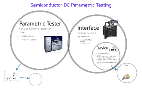


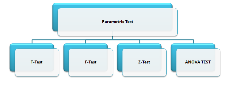


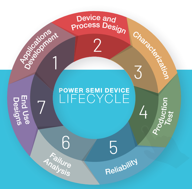

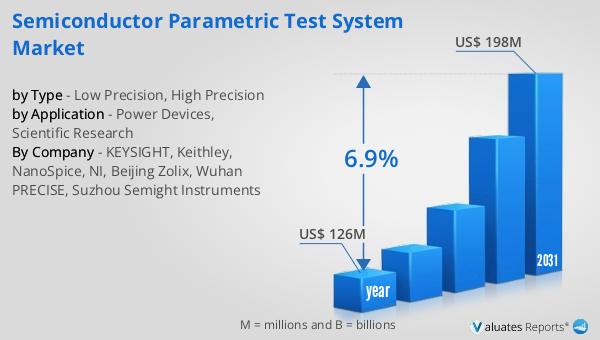
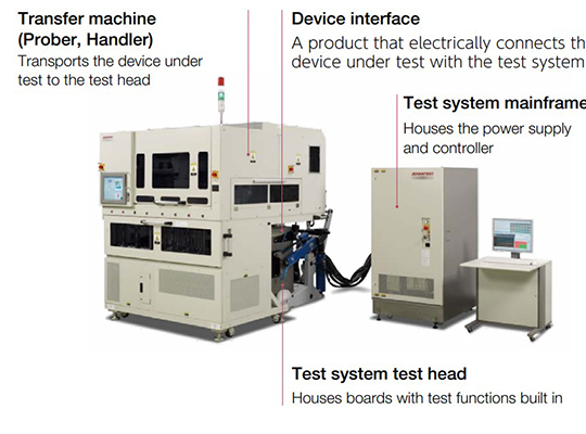


Discover the thrill of accelerating large-scale semiconductor parametric testing using a multi through substantial collections of breathtaking photographs. showcasing the dynamic nature of photography, images, and pictures. designed to inspire exploration and discovery. Browse our premium accelerating large-scale semiconductor parametric testing using a multi gallery featuring professionally curated photographs. Suitable for various applications including web design, social media, personal projects, and digital content creation All accelerating large-scale semiconductor parametric testing using a multi images are available in high resolution with professional-grade quality, optimized for both digital and print applications, and include comprehensive metadata for easy organization and usage. Explore the versatility of our accelerating large-scale semiconductor parametric testing using a multi collection for various creative and professional projects. Diverse style options within the accelerating large-scale semiconductor parametric testing using a multi collection suit various aesthetic preferences. The accelerating large-scale semiconductor parametric testing using a multi collection represents years of careful curation and professional standards. Instant download capabilities enable immediate access to chosen accelerating large-scale semiconductor parametric testing using a multi images. Regular updates keep the accelerating large-scale semiconductor parametric testing using a multi collection current with contemporary trends and styles. Comprehensive tagging systems facilitate quick discovery of relevant accelerating large-scale semiconductor parametric testing using a multi content.