Please enter url.
Login
Logout
Please enter url.
Cmos Inverter Circuit Diagram - Design Talk
design.udlvirtual.edu.pe
source
Comments
Schematic diagram of a CMOS inverter. | Download Scientific Diagram
Bandwidth Extension for Transimpedance Amplifiers | IntechOpen
Schematic diagram of a CMOS inverter | Download Scientific Diagram
The input and output voltage waveforms of CMOS inverter circuit are ...
The measured SAR ADC output noise. | Download Scientific Diagram
Proposed Design using MOSFET | Download Scientific Diagram
Solved: Draw the circuit diagram of a CMOS inverter. Draw its e ...
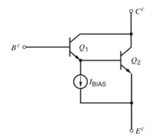
Solved For the Darlington circuit shown below, calculate the | Chegg.com
(a) Single-ended transconductance block, (b) fully differential ...
Schematic representation of an inverter based CMOS SERO with the ...
Gaussian basis circuit. | Download Scientific Diagram
An energy-efficient high-speed CMOS hybrid comparator with reduced ...
Schematic of the clock booster. | Download Scientific Diagram
Bootstrapped NMOS switch | Download Scientific Diagram
The flip flop circuit. | Download Scientific Diagram
Block diagram of the instrumentation amplifier in AE. | Download ...
Conventional ring-amplifier with resistive generated dead-zone ...
Design of Two-stage High Gain Operational Amplifier Using Current ...
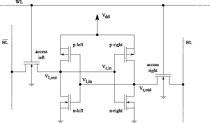
7.3 6T SRAM Cell
4-transistor MOS mismatch structure. | Download Scientific Diagram
ULV floating-gate tanh-shaped transconductance amplifier. | Download ...
Three-transistor dynamic latch. | Download Scientific Diagram
Figure 11 from A Transient-Enhanced Output-Capacitorless LDO With Fast ...
2: A n-input NMOS FG transistor | Download Scientific Diagram
Schematic diagrams of NAND2 gates: (a) IG, (b) IG2, (c) XT, and (d) XT2 ...
(PDF) A Rare Event Based Yield Estimation Methodology for Analog Circuits
Structural Design of CMOS Voltage Regulator for Implantable Devices ...
Equivalent circuit of NC‐CMOS with the FE capacitor connected to the ...
Nanomaterials | Free Full-Text | Ultra-Low-Voltage-Triggered Silicon ...
Figure 2 from A configurable CMOS multiplier/divider for analog VLSI ...
The multidimensional Gaussian circuit. The circuit is shown for 4 ...
The proposed circuit during interval 0 at the second harmonic of the ...
Figure 1 from Design of High Speed Full Adder using Improved ...
Self Assesment Quiz
Explain Clocked CMOS in detail
Inverter-Using-CMOS
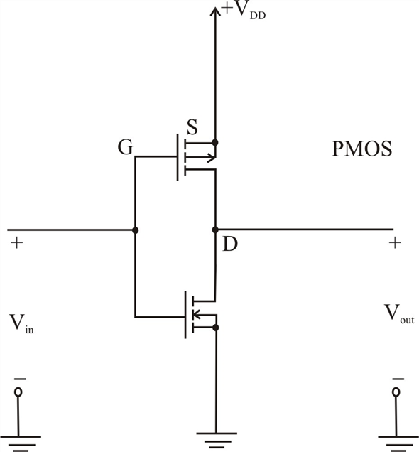
PMOS-Inverter
CMOS-Inverter-Schematic
NMOS-Inverter
Layout-of-CMOS-Inverter
Dynamic-CMOS-Inverter
CMOS-Inverter-Block-Diagram
CMOS-Inverter-VTC
Inverter-Wiring-Diagram
Inverter-Logic-Gate
CMOS-Inverter-Graph
MOS-FET-Inverter
CMOS-Inverter-Truth-Table
CMOS-Inverter-Cross-Section
Inverter-Oscillator-Circuit
Inverter-Gate-IC