Please enter url.
Login
Logout
Please enter url.
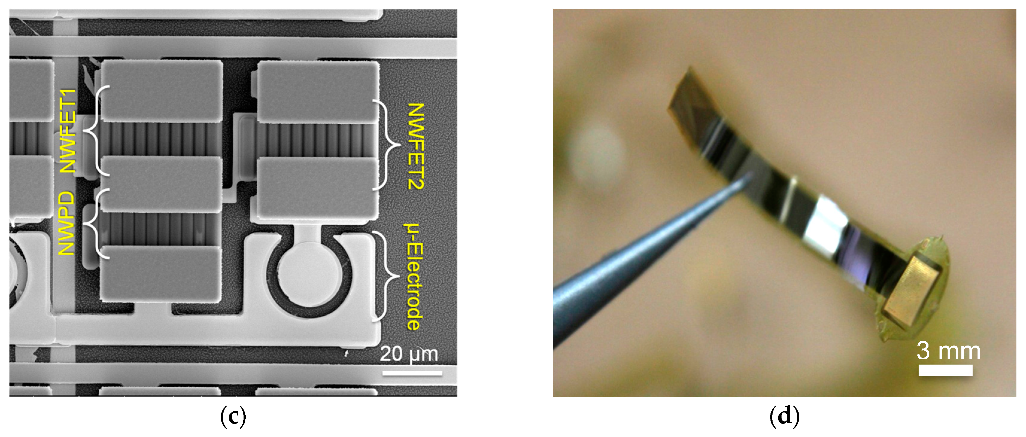
Sensors | Free Full-Text | Neuron Stimulation Device Integrated with ...
mdpi.com
source
Comments
The wafer-scale photonic Damascene process flow and highlighted ...
(PDF) Superconducting Qubits and Quantum Resonators
Images of finished tunable HCG-VCSEL devices. (a) Scanning electron ...
(PDF) 3D Integrated Laser Attach Technology on 300-mm Monolithic ...
Details of the fabricated meta-device. SEM magnification of (a) the ...
(a) Microscopy image of the MZI structure of the Si/TFLN modulator. (b ...
The micro fastener images: (a) side view observed by optical ...
(a) Overall representation of the proposed EIS system. (b) Overall ...
Energy deposition for alpha particles, tritons, deuterons and protons ...
(PDF) Ultra-high Q/V hybrid cavity for strong light-matter interaction
Relationship of the magnetic flux density and the gap distance between ...
Schematic and picture of “ring trap”. (a) Schematic of a ring trap. The ...
MEMS grating optical filter-controlled dual-color laser Excitation ...
(PDF) Integrated phased array for wide-angle beam steering
(a) SEM image of a Si substrate with a V-groove and Au micro-bumps; (b ...
15 (a) SEM image of nanoimprinted grating EOS MEMS device. (b) Optical ...
Figure 1 from The development of the package of the Terahertz ...
Two examples of NbN thin film thermometers at the millimeter or ...
3-D self-assembled MEMS: a) flow sensor, b) thermal actuator ...
Design of Coplanar Power Amplifiers for Millimeter-wave System ...
(PDF) Historical perspectives, challenges, and future directions of ...
(a) Optical and (b) SEM micrographs of metal patterns after RDL process ...
Electronically Tunable Distributed Feedback (DFB) Laser on Silicon ...
Figure 5 from Wafer-level vacuum sealing and encapsulation for ...
The fabricated gold lamellae layer structures. (a) SEM image of the 7 ...
Schematic of SiNWs embedded pressure with groove and rib structures on ...
COF assembly using WLP with pre-applied ACF (a) ACF lamination on a ...
Sensors | Special Issue : Surface Acoustic Wave and Bulk Acoustic Wave ...
Smallest logic circuit fabricated with single-electron transistors ...
(PDF) Theorical and experimental study of plasmonic metamaterials for ...
Figure 3 from Promoting Chip Probing Test Yield By Simple ISSG and ...
(a) A photograph of the fabricated tactile sensor with hemispherical ...
Fabrication of multi-material 3D structures by the integration of ...
a) Multiple exposures picture of a VO2‐coated silicon cantilever during ...
Scanning electron microscopy images of FIB milled cross-sections ...
Silicon-Nanowires
Photodetector-Image
Nanowire-Transistor
Carbon-Nanowires
Ultraviolet-Photodetector
Silver-Nanowires
MoS2-Photodetector
Nanowire-FET
Flexoelectricity
Solar-Blind-Photodetector
Photodetector-Diagram
Light-Detector
Photodetector-Arrays
Organic-Photodetector
UV-Photodetector
Flexible-Photodetector