


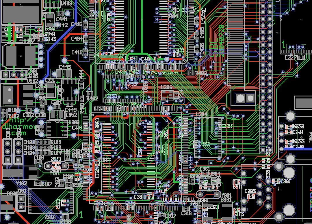


Discover the vibrancy of city life through hundreds of urban convert schematic diagram to pcb layout photographs. showcasing the architectural beauty of photography, images, and pictures. perfect for city guides and urban projects. Our convert schematic diagram to pcb layout collection features high-quality images with excellent detail and clarity. Suitable for various applications including web design, social media, personal projects, and digital content creation All convert schematic diagram to pcb layout images are available in high resolution with professional-grade quality, optimized for both digital and print applications, and include comprehensive metadata for easy organization and usage. Discover the perfect convert schematic diagram to pcb layout images to enhance your visual communication needs. Cost-effective licensing makes professional convert schematic diagram to pcb layout photography accessible to all budgets. The convert schematic diagram to pcb layout archive serves professionals, educators, and creatives across diverse industries. Multiple resolution options ensure optimal performance across different platforms and applications. Professional licensing options accommodate both commercial and educational usage requirements. Whether for commercial projects or personal use, our convert schematic diagram to pcb layout collection delivers consistent excellence. Advanced search capabilities make finding the perfect convert schematic diagram to pcb layout image effortless and efficient. Comprehensive tagging systems facilitate quick discovery of relevant convert schematic diagram to pcb layout content.