Please enter url.
Login
Logout
Please enter url.
cpu transistor under microscope - scoala-de-soferi.ro
scoala-de-soferi.ro
source
Comments
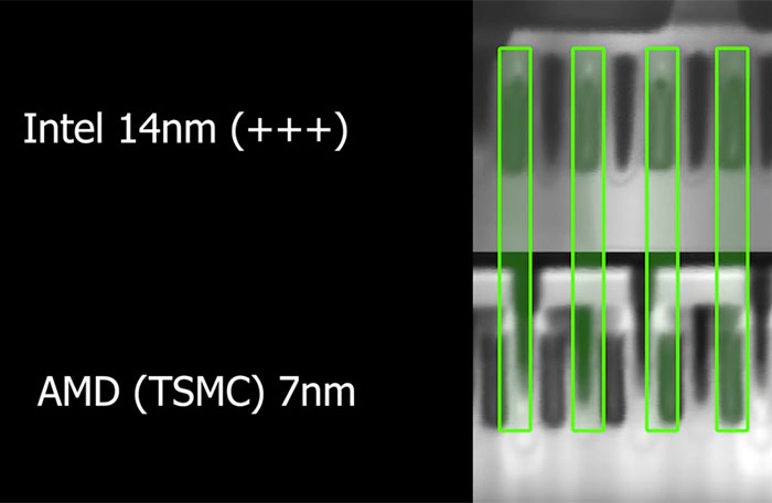
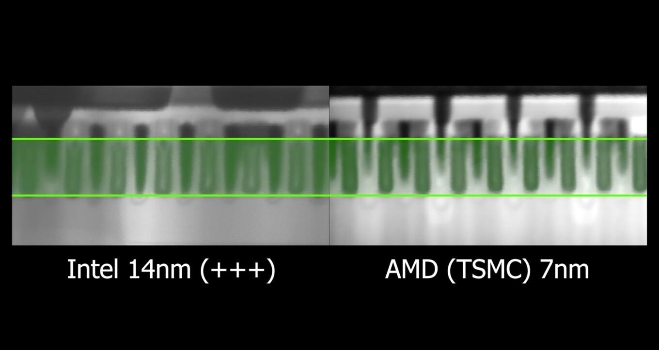
Intel 14nm and AMD/TSMC 7nm transistors micro-compared - CPU - News ...
Back-scattered electron images of the cross-sections of the SiC/TAD ...
(a) schematic under CADENCE of a simple MRAM memory cell composed of a ...
Electronics | Teledyne DALSA
Validation result of a read operation for a 1T1C FeRAM memory cell for ...
CMOS Charge-Domain Global Shutter Pixel IP – Photolitics
FIB cross section SEM demonstrating remaining silicon thickness of ...
Micrograph of a fabricated chip in the 65 nm CMOS process. | Download ...
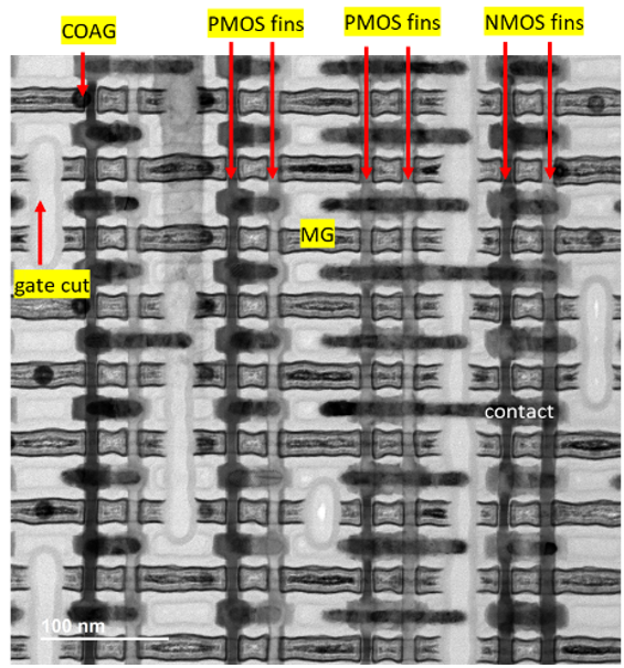
Cross section TEM of NS structure showing source/drain epi with high ...
(a) PCMS, the vertically integrated memory cell of one PCM and one OTS ...
Microscopy Solutions for Analog, RF, Power, MEMS, and Sensors
Intel 14 nm Node Compared to TSMC's 7 nm Node Using Scanning Electron ...
Thermal Imprint System | Thermal Imprint System | Film-Production ...
Reconstruction of captured hologram. The reconstructed image has a size ...
1 a filtered HRTEM micrograph showing a coherent transition region ...
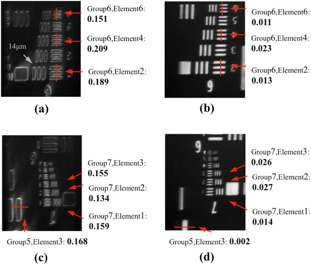
2D MTF graph derived from the Siemens star image. As the electron spot ...
Localization and shaping of surface acoustic waves using PDMS posts ...
SEM micrographs of large Si-nanowire arrays (100 × 100) after their ...
Florian Eisenhardt posted on LinkedIn
Wafer Prep Key To Thinning SiP
Integrated Photonics Research Group (Mookherjea)
Figure 1 from Improving Tungsten gap-fill for advanced contact ...
Examination of antigen expression and antibody binding. U266 multiple ...
Scanning electron micrographs of photoresist nanoposts created by two ...
Images of the USAF resolution target reconstructed from the correlation ...
Amplitude of THz emission from photoexcitation of an integrated circuit ...
An SEM image of a prototyped 1 : 3 power splitter. | Download ...
Inspection of 01005 components now standard in OptiCon AOI systems
PS –We don’t need EUV! - BetaBlog
Library size measurement by E-gel®. The average size for all the ...
Shyh-Chiang Shen – ECE Professor
JSR and IBM low-k JDPs for 32/22nm - BetaBlog
Revealing the Hidden Innovations within the A15 Bionic SoC
Fast 3D imaging in optical microscopy
Physicochemical, enzymatic and molecular characterisation of the ...
Transistor-Size
Transistor-Size-Chart
First-Transistor-Size
Transistor-Size-by-Year
Evolution-of-Transistor-Size
Transistor-Size-Over-Time
Smd-Transistor-Size-Comparison
Transistor-Count
Transistor-Size-Gra
Microprocessor-Transistor-Size
Decrease-of-Transistor-Size
What-Is-the-Size-of-a-Transistor
Transistor-Types
Size-of-a-Transistor-On-a-Supercomputer
Transistor-History
Transistor-Size-22Nm