Please enter url.
Login
Logout
Please enter url.
Cross-sectional (left) TEM and (right) elemental EDS mapping images of ...
researchgate.net
source
Comments
(a) Θ−2 Θ x-ray diffraction pattern and (b) φ-scans on STO (101) and ...
[(a)-(d)] EDX elemental mapping of four chemical species (Au, Ti, O ...
Layer wise chemical mapping examined by point analysis of EDX spectra ...
(a) STEM micrograph and EDS elemental maps of (b) Pt, (c) Sn, and (d ...
Heterojunction oxide thin-film transistors with unprecedented electron ...
EDX spectrum of the prepared silver-integrated silica nanostructures ...
EDX intensity profile a and the SEM image b of the p-NOC after reacted ...
(a) HAADF image of the grain boundary. EELS data were collected from ...
A two-step chemical vapor deposition process for the growth of ...
a HAADF, b–e elemental Map, and f EDS analysis of the powders ...
Top panel: EELS survey spectrum showing the K-edge absorption features ...
Identification and classification of particle contaminants on ...
(a) Crystal structure of Mn3Ir. (b) The AFM structures characterized by ...
SEM image, EDX spectrum, and elemental mapping images of GO-Fe 3 O 4 ...
Microorganisms | Free Full-Text | Limonin Enhances the Antifungal ...
(PDF) Oxygen vacancy enhanced room-temperature ferromagnetism in Sr3SnO ...
(PDF) Lanthanide-Doped Core-Shell-Shell Nanocomposite for Dual ...
XPS spectra of a In0.5Sc1.5Mo3O12, b In 3d peaks, c Sc 2p peaks, d EDX ...
(a) On-axis XRD around the 220 substrate reflection and (b) an ...
Membranes | Free Full-Text | Impact of Physical and Chemical ...
(A) TEM of converted-ALD MoS 2 on silicon converted at a temperature of ...
(a) XRD patterns and (b) average Raman spectra of Sb 2 O 3 /N-GNR and ...
Characterization of ER-Au/Ag NCs. a Representative TEM image of ...
Structural, chemical profiling of the Si/GaP-TiO 2-MoS 2 photocathode ...
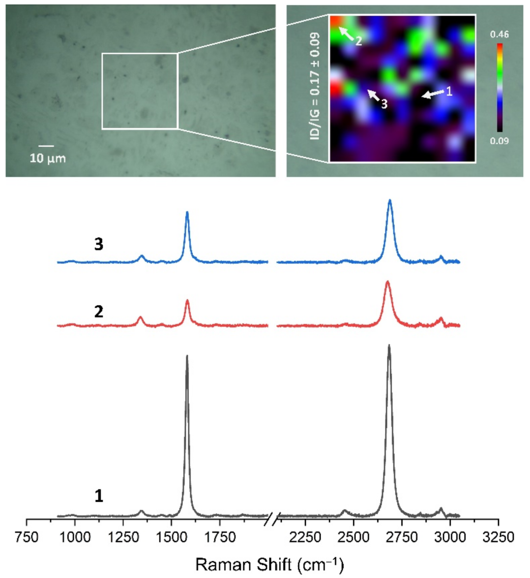
Single point (a) Raman and (b) photoluminescence spectra before and ...
(a) Subdiffraction resolution STED image and (b) corresponding ...
Materials | Free Full-Text | Atomistic Construction of Silicon Nitride ...
(a) Streak camera data showing the time-resolved PL emission at 5 K ...
Membranes | Free Full-Text | Impact of Physical and Chemical ...
The growth process of the FAPbI3 perovskite film. a) The areal ...
Lithium-ion transport in inorganic active fillers used in PEO-based ...
SEM image, elemental mapping and elemental point analysis of La, Ni ...
RHEED images of the top Ni and Cu layers along the 100 direction of ...
(a) XRD patterns of undoped LSMO and all Co-doped LSMO samples. (b) and ...


![[(a)-(d)] EDX elemental mapping of four chemical species (Au, Ti, O ...](https://www.researchgate.net/publication/330819927/figure/fig5/AS:11431281107422317@1671040441688/a-d-EDX-elemental-mapping-of-four-chemical-species-Au-Ti-O-and-Ga-e-EDX.png)