Please enter url.
Login
Logout
Please enter url.
Details of FEM modeling of (a) direct bumped on the Cu/low-k stack and ...
researchgate.net
source
Comments
(a) Optical and (b) SEM micrographs of metal patterns after RDL process ...
Structure and SEM images of CNT placement, device, and ring oscillator ...
Direct Cu to Cu Bonding and Other Alternative Bonding Techniques in 3D ...
(a) The working principle of the tilt-beam CD-SEM. The feature of ...
(a) Far field images of slow steering show steering throughout the ...
(a) An optical microscope image of metal contacts (patterned using ...
(a)-(e) Schematic illustrations of the growth of GaN islands with ...
3: (A) Schematic diagram illustrating multiple steps to fabricate phase ...
(Color online) Device schematic diagram, scanning electron micrographs ...
(a) Optical image of a completed device with multiple Hall bar ...
Thermal and quantum phase slips in niobium-nitride nanowires based on ...
Proceedings | Free Full-Text | Fabrication of Planar Copper Microcoils ...
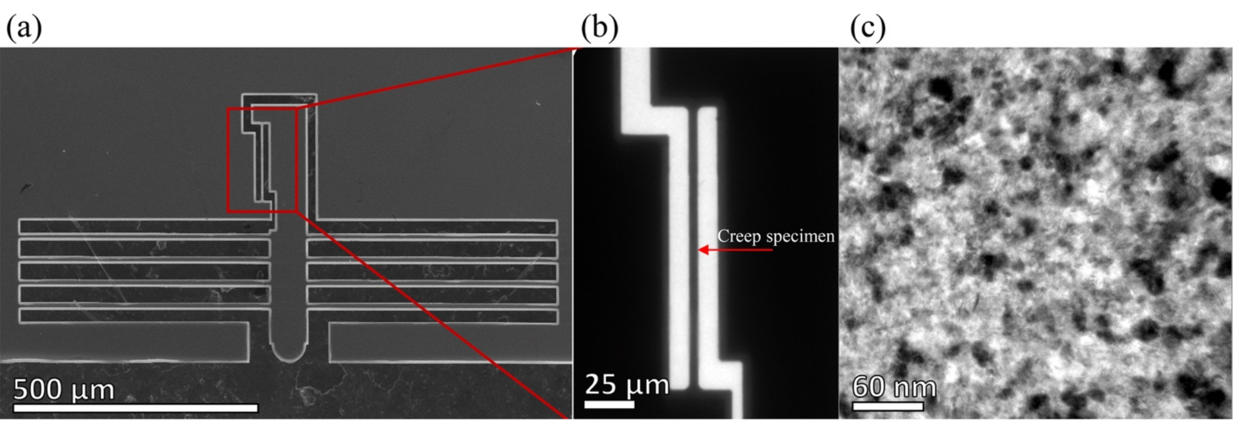
Array of nanomechanical resonators. SEM images of 5×4 NEMS array used ...
(a) Top view of multiple fin array of InAs grown uniformly from Silicon ...
SEM images of the fabricated plasmonic PCA, illustrating its major ...
(a) Process for transfer of polyimide films by rolling [195] and (b ...
(a)–(h) General process steps needed to fabricate test structures ...
The optical micrograph image (a) and corresponding SEM image (b) of a ...
(a) Fabricated structure for phase-changing of thin GST film with ...
(a) Schematic of the M-ZI. (b) The cross-sectional schematic of the ...
(a) Scanning electron microscope (SEM) image of a Si nanostructure ...
Micromachines | Free Full-Text | A Thermopile-Based Gas Flow Sensor ...
(PDF) Dynamic control of the asymmetric Fano resonance in side-coupled ...
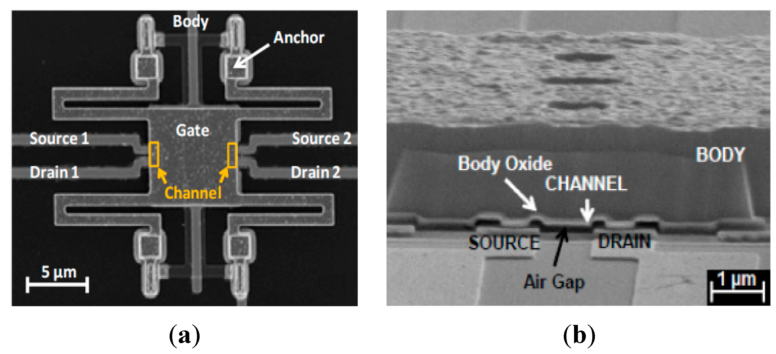
Micromachines | Free Full-Text | Nanoelectromechanical Switches for Low ...
Eight‐wavelength hybrid Si/AlGaInAs/InP microring laser array - Sui ...
Tilted view SEM images after release of stacked NW. (a) Schematic of ...
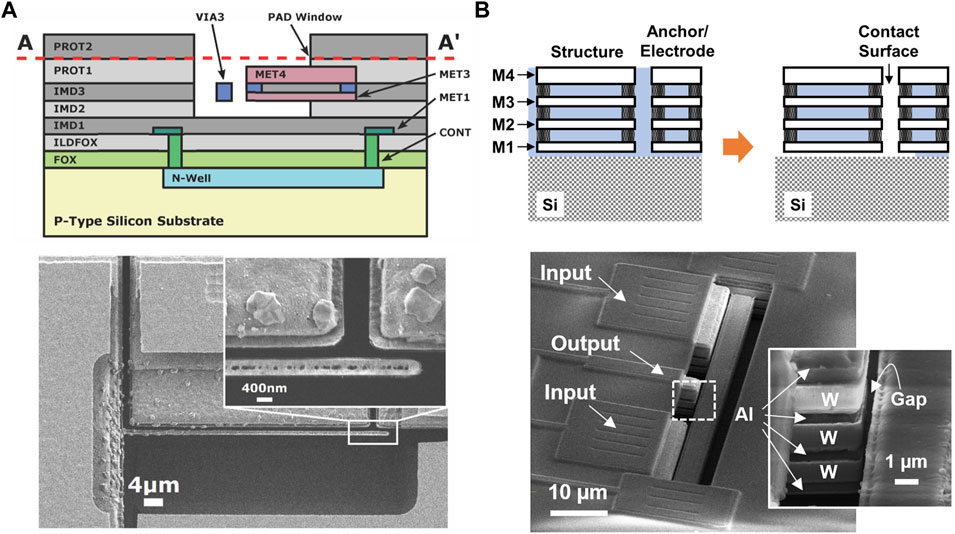
Figure 1 from TSV Integration With Chip Level TSV-to-Pad Cu/SiO₂ Hybrid ...
(a) Microscope image of top-view and (b) FIB image of cross-sectional ...
Free Ebook: The Latest Development Trends in CMOS Image Sensors - F4News
Stretchability of a fabricated pressure sensor network. (a) Top view of ...
Electronics | Free Full-Text | Development of Temperature Sensor Based ...
Figure 2 from Impact of TSV process on 14nm FEOL and BEOL reliability ...
Scanning electron microscopy images of FIB milled cross-sections ...
Frontiers | CMOS-MEMS Vibro-Impact Devices and Applications
Sample Preparation and Experimental Design for In Situ Multi-Beam ...