Please enter url.
Login
Logout
Please enter url.
Proceedings | Free Full-Text | Analysis of pn Junction Deep Trench ...
mdpi.com
source
Comments
(PDF) Real-Time DC-dynamic Biasing Method for Switching Time ...
µTP of LN with a different pillar design: (a) Optical microscope image ...
Figure 2 from Photonic Damascene Process for Low-Loss, High-Confinement ...
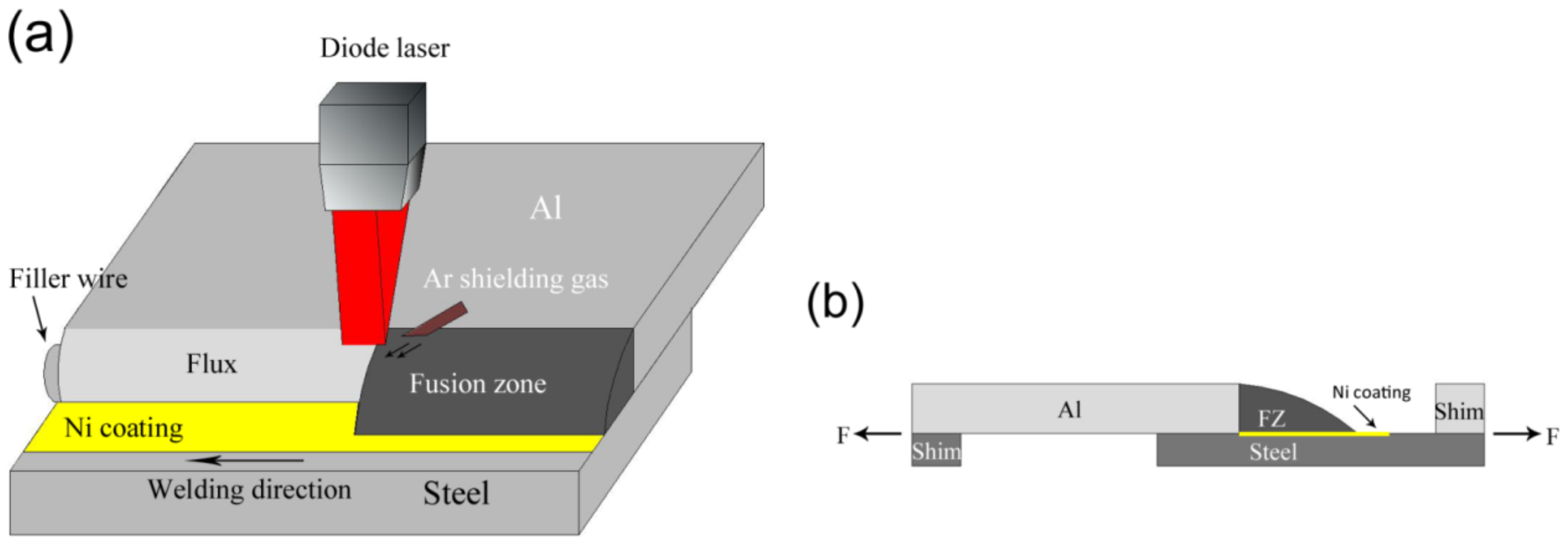
Applied Sciences | Free Full-Text | Diode Laser Welding/Brazing of ...
Assembling process of the proposed sensor. (a,b) bonding of PDMS layers ...
Biosensors | Free Full-Text | Advances in Microfluidics for Single Red ...
(a) Current versus voltage for FCLEDs with Ag/TiW and ITO/DBR. (b ...
Fabrication procedures of the developed sorter. Molds were made using ...
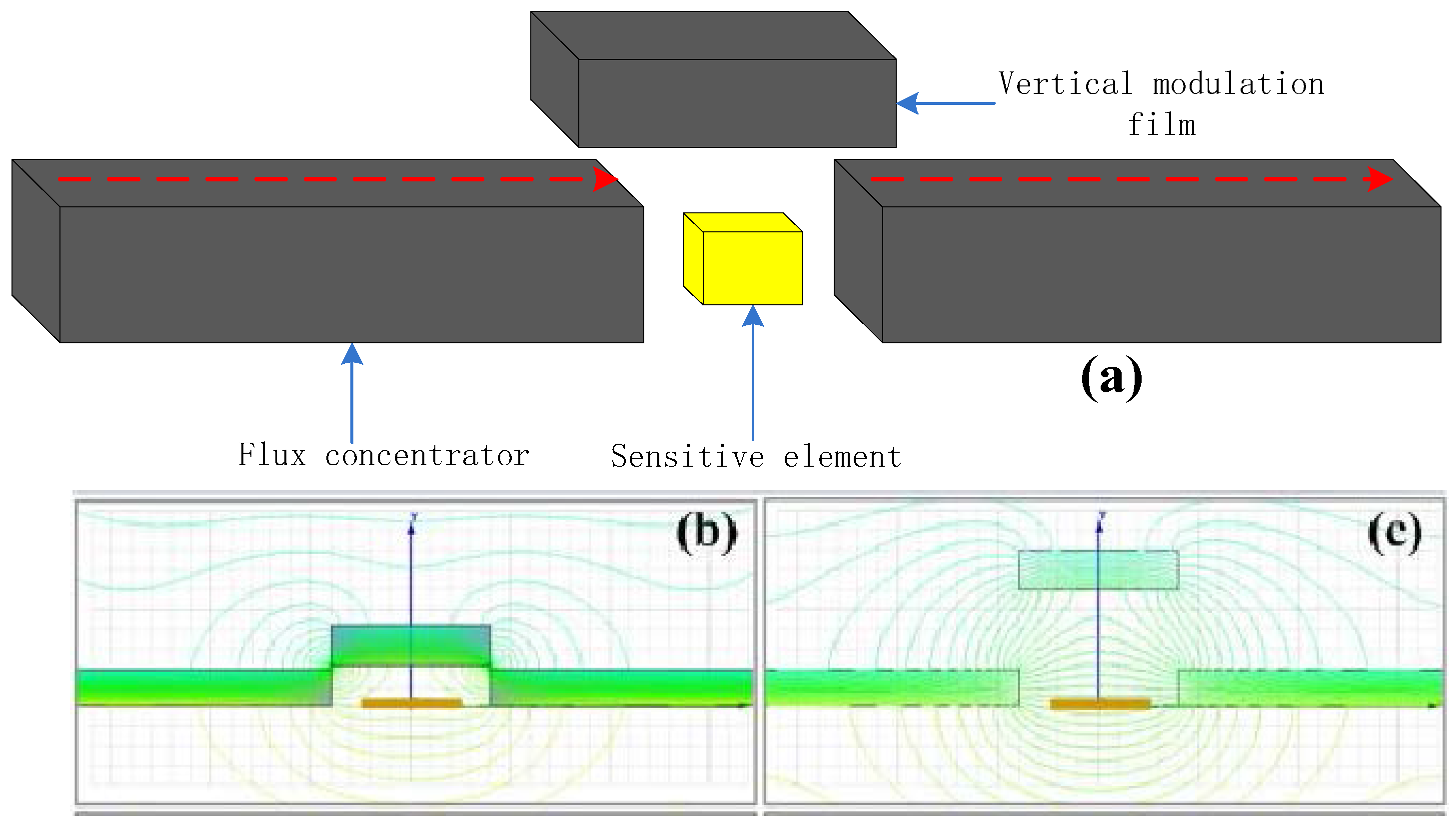
Micromachines | Free Full-Text | A Novel High-Precision Digital ...
Nanomaterials | Free Full-Text | Enhanced Reflection of GaAs Nanowire ...
a Schematic of bonding process, b interfacial layer of bonded Co/Sn/Co ...
Frontiers | Silicon photonic integration in telecommunications
Tip sharpness and durability assessment of the LSNT-tip SU8 cantilevers ...
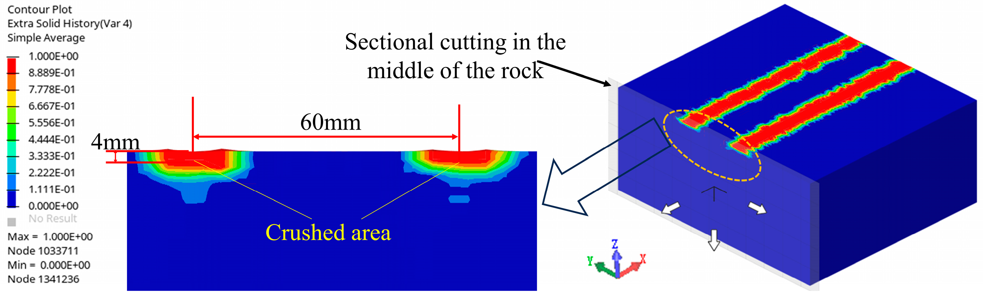
Applied Sciences | Free Full-Text | A Study on the Rock-Breaking ...
(a) Schematic of the butt TIG welding for joining the aluminum to steel ...
Figure 1 from A noble VFO(Vertical wire Fan Out) technology for small ...
Materials | Free Full-Text | Process-Related Changes in Polyetherimide ...
Interdigitated electrodes fabricated by photolithography and lift-off ...
Technology Consulting Services
Microcantilever fabrication process: (a) membrane photolithography, (b ...
[PDF] Top-down fabrication of sub-30 nm monocrystalline silicon ...
Figure 1 from Self-aligned Metal Double-gate P-channel Low-temperature ...
Schematic of the fabrication process of a silicon nanowire FET sensor ...
(a) Schematic of the integrated half-ridge PC, (b) Cross-section image ...
研究成果 - 李 菲 - 教师个人主页
Antennas for Body Centric Wireless Communications at Millimeter Wave ...
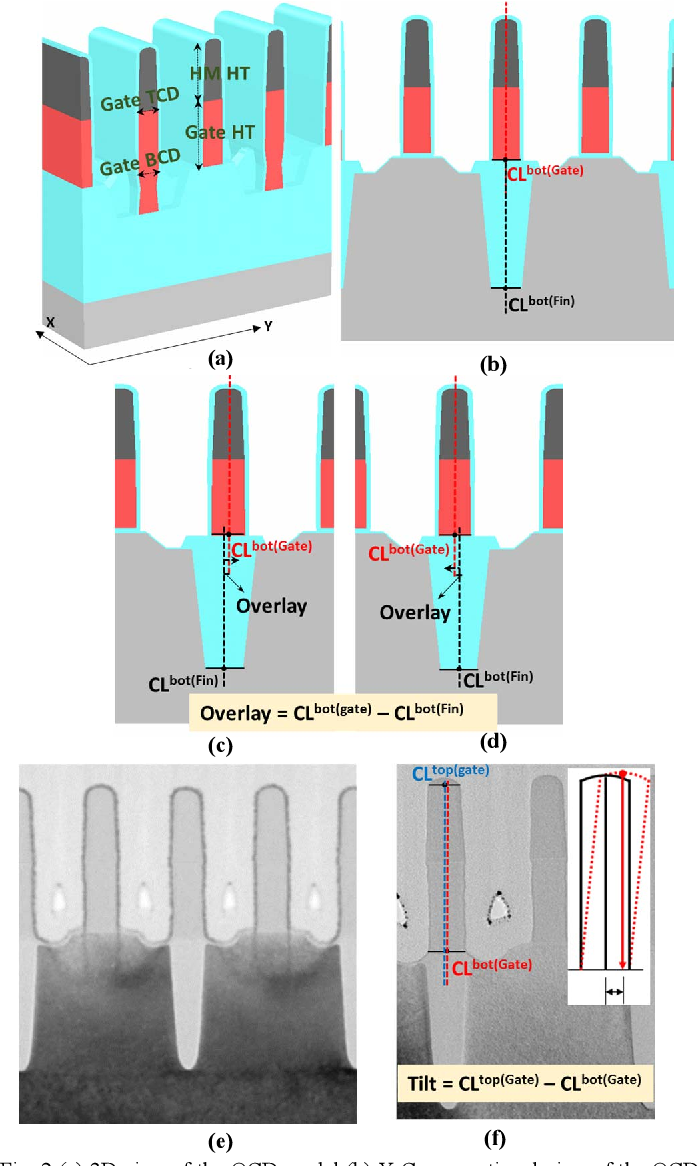
Figure 2 from Characterization of Overlay and Tilt in Advanced ...
Inversely tapered edge-coupler. (a) Top view SEM image of the ...
Silicon surface patterning via galvanic microcontact imprinting ...
(a) Cartoon showing the bump-shear test on a signal pillar. (b) SEM on ...
Fundamentals of Thermal Compression Bonding Technology and Process ...
Technologies and challenges of fine-pitch backside via-last 3DIC TSV ...
Origami-based electrochemical impedance spectroscopy assay for ...
Helium ion beam milling for plasmonic nanoantennas


![[PDF] Top-down fabrication of sub-30 nm monocrystalline silicon ...](https://d3i71xaburhd42.cloudfront.net/1ebcdcc44c8bd9767333f46f081225916fe26ffb/2-Figure1-1.png)