Please enter url.
Login
Logout
Please enter url.
PCB布局的芯片上,跳过包和加入的乐趣 - beplay软件下载ios
ulabos.com
source
Comments
FlipChip Package Overview - AnySilicon
FAQ-FlipChip Nov
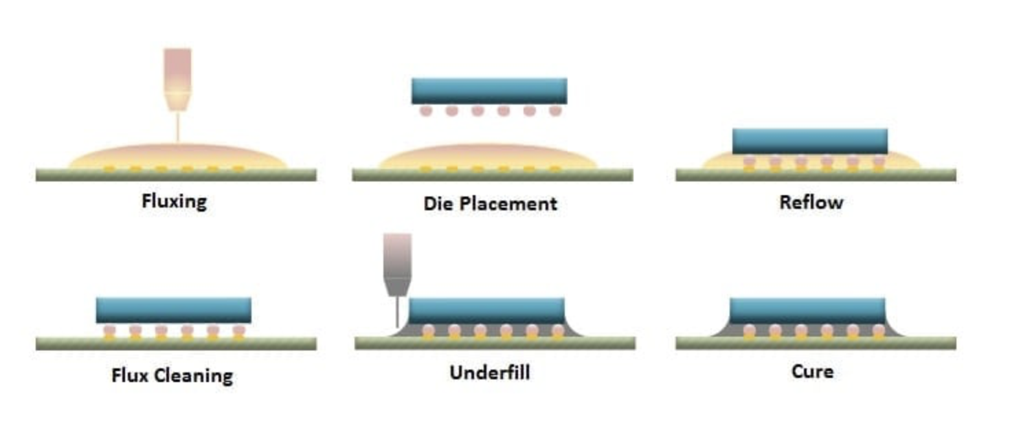
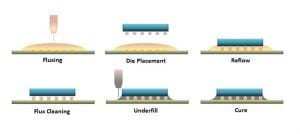
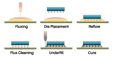
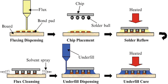
Flip-Chip Underfill: Materials, Process, and Reliability | SpringerLink
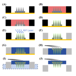
Neural Interfaces | Utah Nanofab
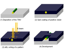
Nanotechnology: Electron beam lithography scheme suits tobacco mosaic ...
Step-by-step typical process flow for heterogeneously integrated III-V ...
Main process steps in BEOL processing and possible variations ...
Fan in Vs Fan out WLP The RDL technology is to convert the welding area ...
(PDF) Memristor Fabrication Through Printing Technologies: A Review
AI Expansion - Supply Chain Analysis For CoWoS And HBM
Cross-Section of Fermilab Test Chip Assembly | Download Scientific Diagram
Figure 3 from Stress Studies to Optimize the FCBGA Bumping Structure ...
(PDF) Underfill Flow in Flip-Chip Encapsulation Process: A Review
The schematic diagrams illustrating different solution‐fabrication ...
Figure 1 from Morphology and Mechanical property of Cu pillar formed by ...
Flip-Chip Underfill: Materials, Process, and Reliability | SpringerLink
Flip-Chip Underfill: Materials, Process, and Reliability | SpringerLink
(PDF) Fine Line Routing and Micro Via Patterning in ABF Enabled by ...
Laser capture microdissection system technology – In the top panel (a ...
A fabrication process flow for creating CVD diamond hemispherical shell ...
Principle (a) and flowchart (b) of laser shock hole-clinching process ...
Figure 2. Fabrication flow of the PZT pyroelectric cell. | Scientific ...
5: Illustration of positive photolithography and lift o↵ after metal ...
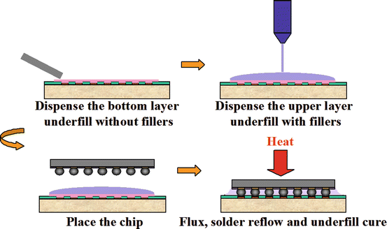
A multi-layer wafer-scale underfill process | Download Scientific Diagram
Integration of Plasmadust ® step after solder paste printing (above ...
Process steps for building an electrochemical transistor. Patterning of ...
Canon to build nanoimprint factory to challenge ASML
General Wet Etch (Left) vs. KOH Etch (Right) | Download Scientific Diagram
Oxygen insensitive thiol–ene photo-click chemistry for direct imprint ...
Electronics | Free Full-Text | Die-Level Thinning for Flip-Chip ...
Thick copper paves way for high-current drive in high-voltage power ICs ...
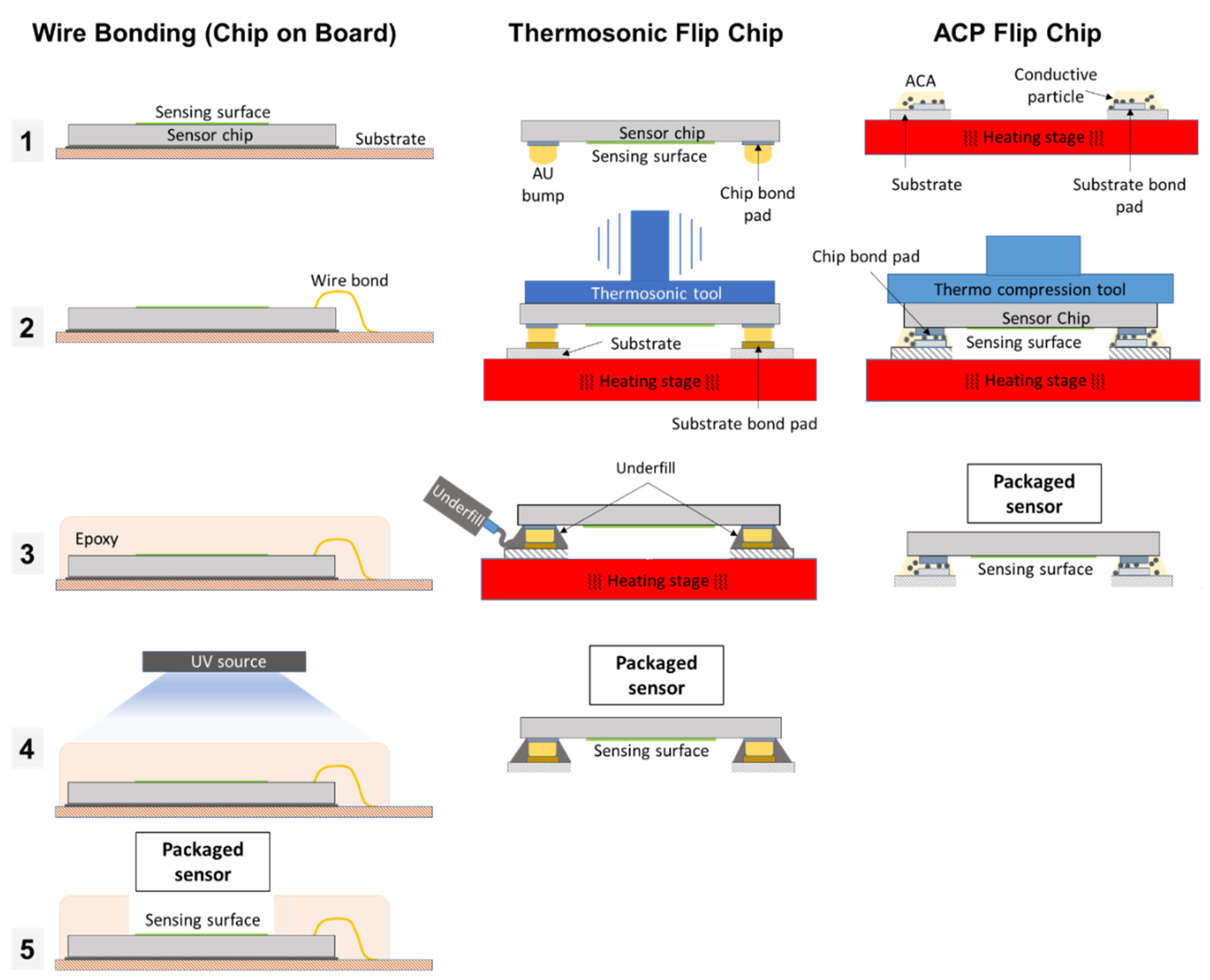
The development of Anisotropic Conductive Paste (ACP) to make solder ...
Freeze frame: JSR closes in on double patterning at 22nm - Document ...
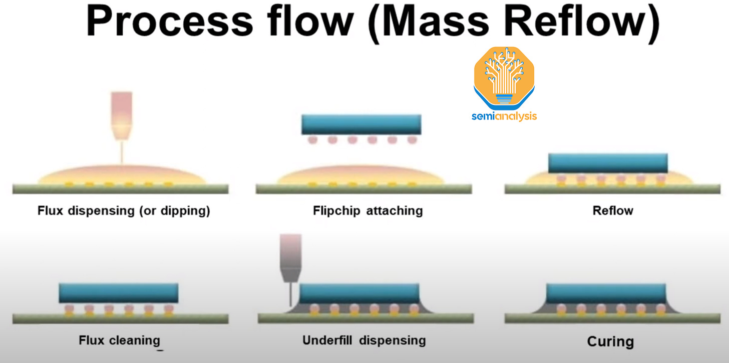
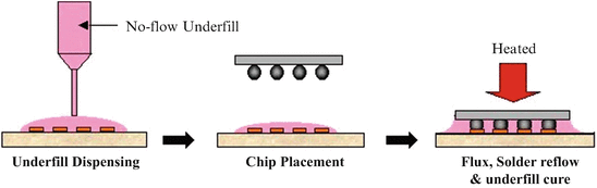
Void free processing of flip chip on board assemblies using no-flow ...
Die Attach Pastes | Die Attach Materials | CAPLINQ Corporation
LED-On-Board
Circuit-Board-Chips
Chip-On-Board-LED
Cob-Package
Chipboard
Notice-Board-Chip-Board
IC-Chip
Silicon-Die
Perf-Board-IC-Chips
Chipboard-Computer
ZN1-Chip-Board
IC-Chip-Design
Flip-Chip-Packaging
Computer-Board-Chips-E-Scrap
Chip-and-Wire-Assembly
Chipset