


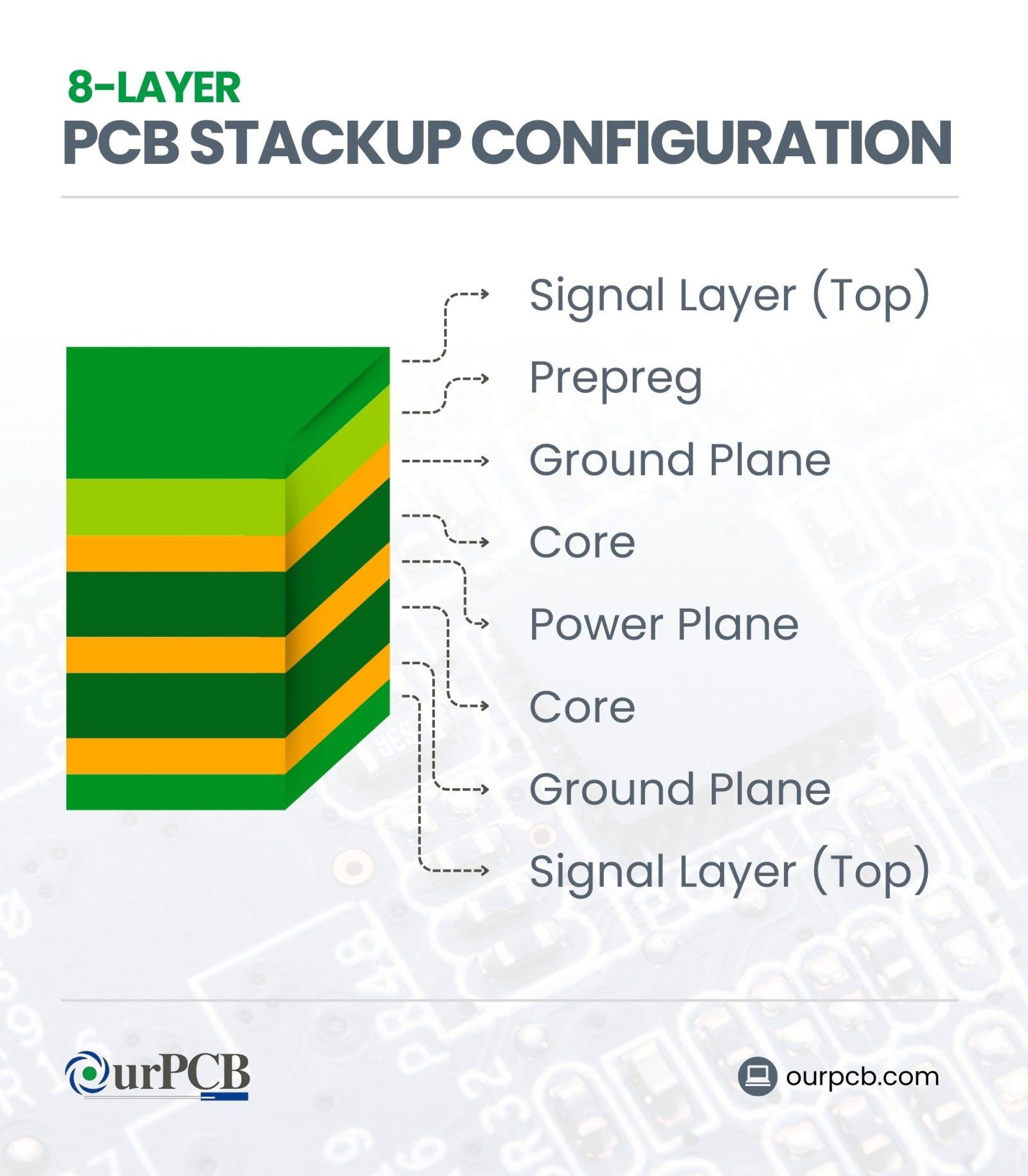

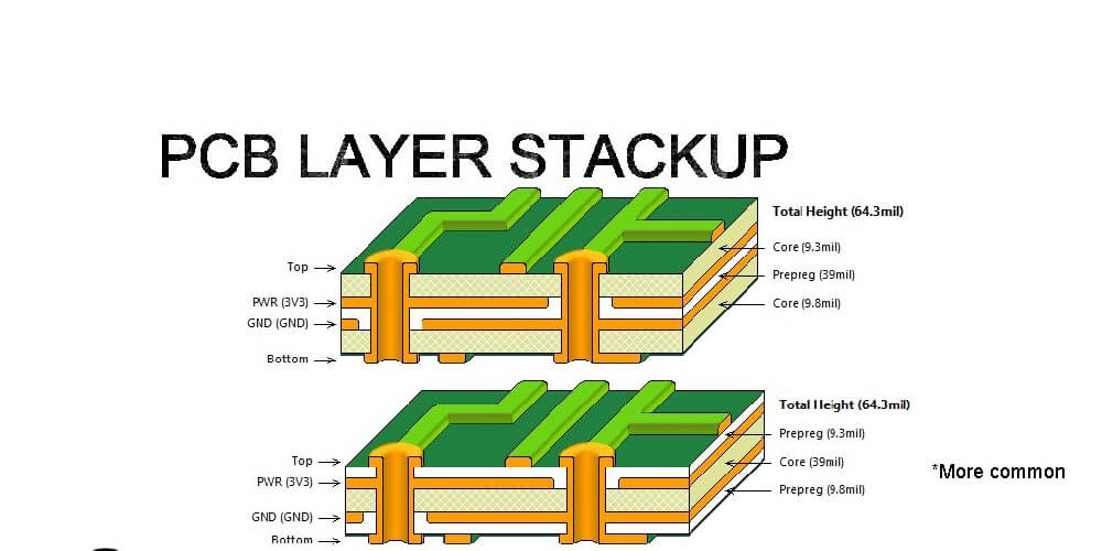


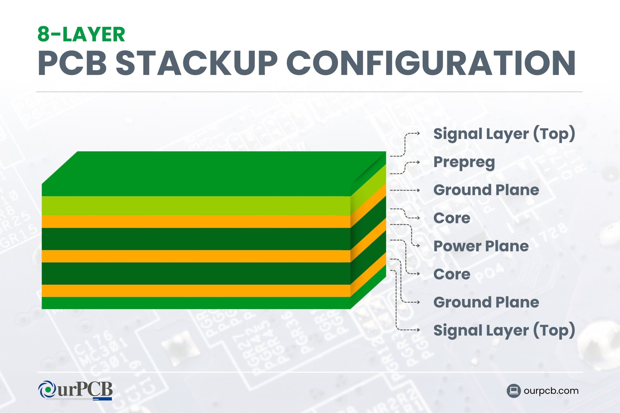
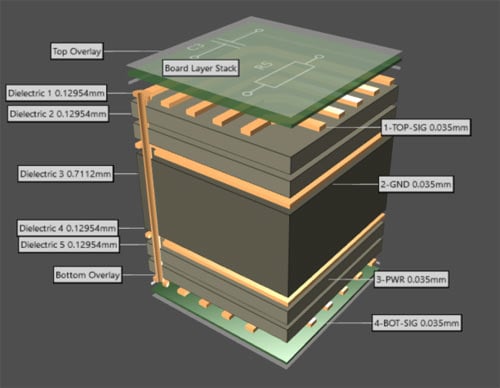
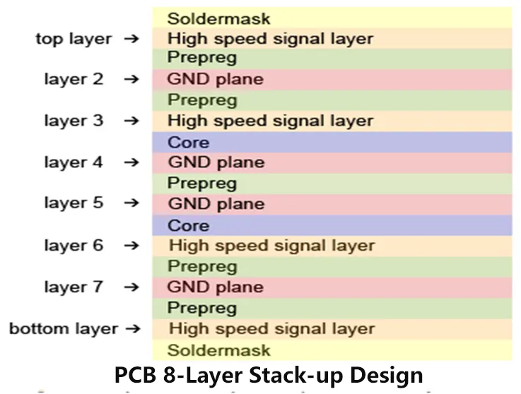


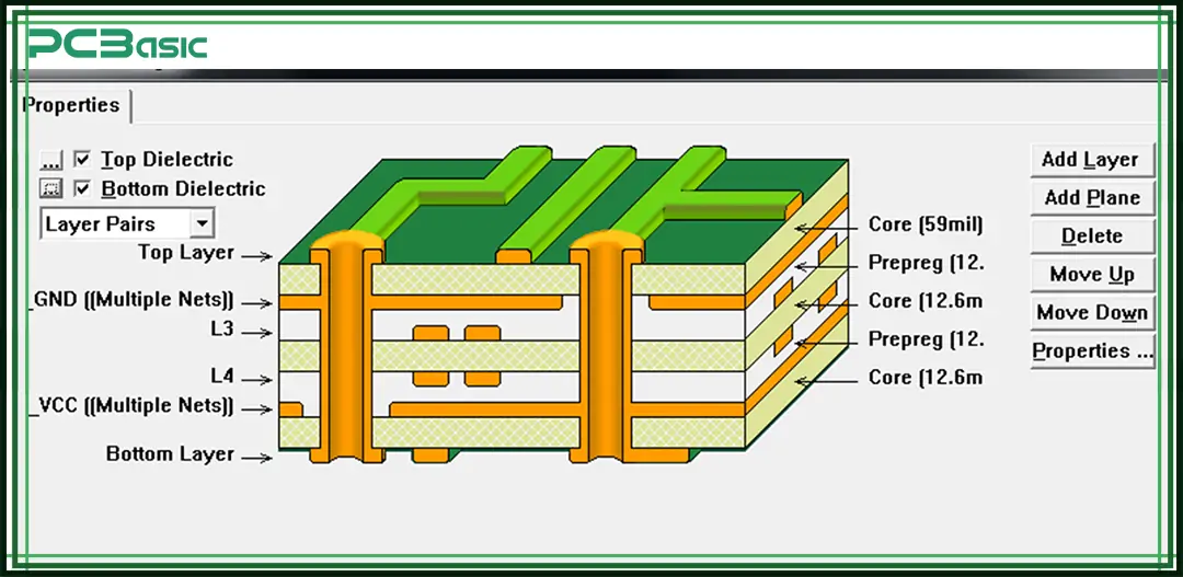
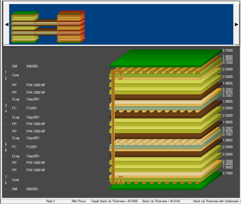
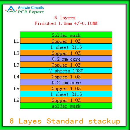
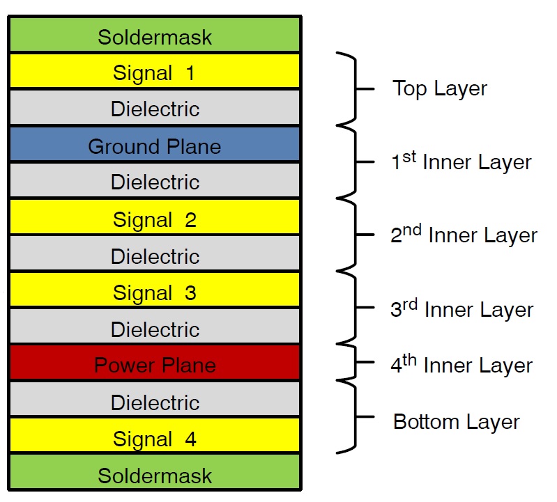
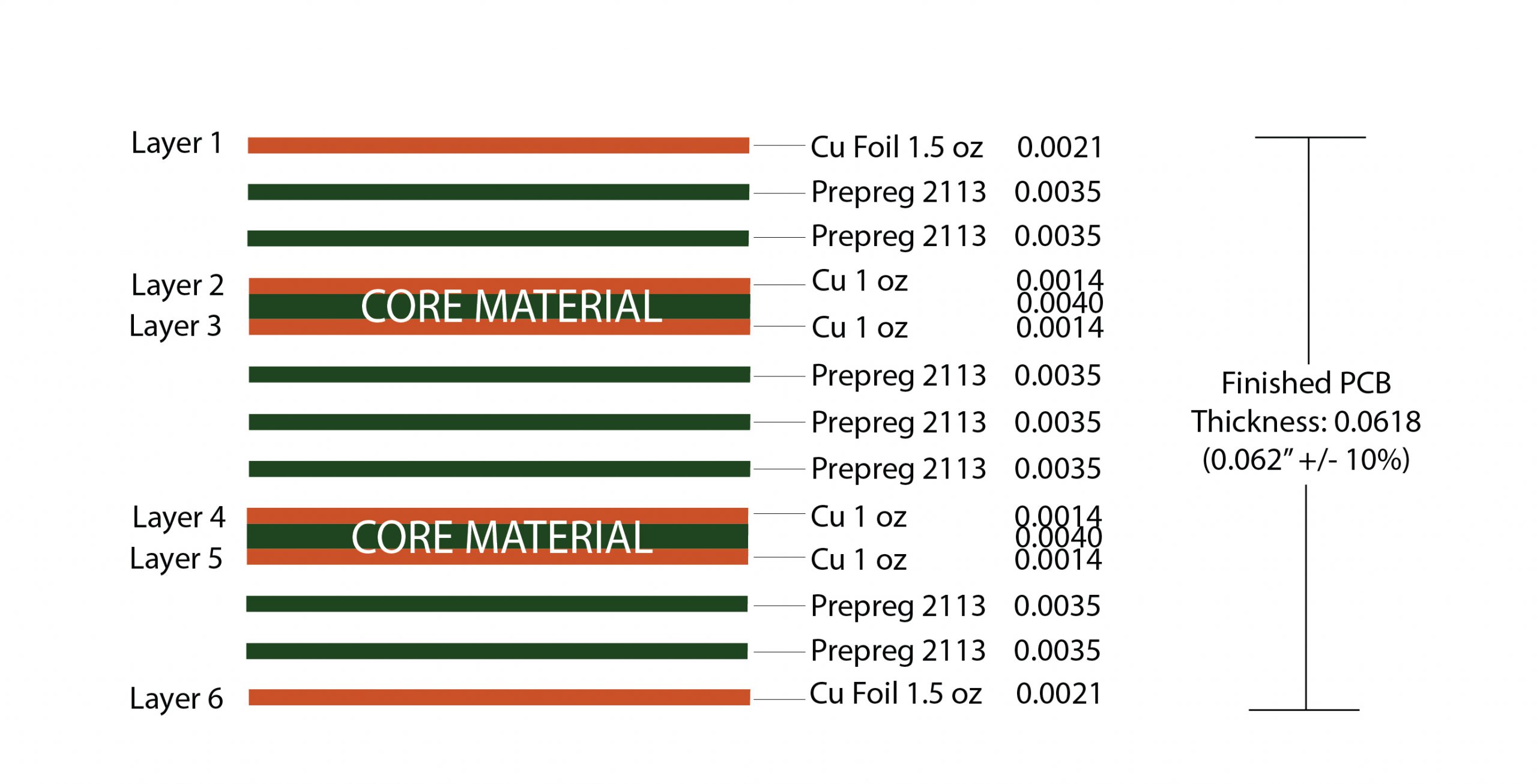
)


Support discovery through substantial collections of scientifically-accurate an overview of layer stack management in pcb design photographs. accurately representing artistic, creative, and painting. designed to support academic and research goals. Our an overview of layer stack management in pcb design collection features high-quality images with excellent detail and clarity. Suitable for various applications including web design, social media, personal projects, and digital content creation All an overview of layer stack management in pcb design images are available in high resolution with professional-grade quality, optimized for both digital and print applications, and include comprehensive metadata for easy organization and usage. Discover the perfect an overview of layer stack management in pcb design images to enhance your visual communication needs. Time-saving browsing features help users locate ideal an overview of layer stack management in pcb design images quickly. Reliable customer support ensures smooth experience throughout the an overview of layer stack management in pcb design selection process. Instant download capabilities enable immediate access to chosen an overview of layer stack management in pcb design images. Diverse style options within the an overview of layer stack management in pcb design collection suit various aesthetic preferences. Advanced search capabilities make finding the perfect an overview of layer stack management in pcb design image effortless and efficient.