Please enter url.
Login
Logout
Please enter url.
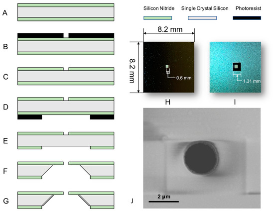
(A-G) Fabrication process for the dielectric film with a single ...
researchgate.net
source
Comments
Micromachines | Special Issue : Micro/Nanofluidic Devices for Single ...
Ultrathin tin sulfide field-effect transistors with subthreshold slope ...
(a) Photograph of the packaged SiNWs-FET chip. (b) Optical microscopy ...
(a) Fabrication process for the S1 Lamb mode resonator. (b) SEM of the ...
Research – Dan Zhao’s Group at NUS
(PDF) Proximity effect in PbTe-Pb hybrid nanowire Josephson junctions
SEM images of specimen fabricated by FIB. | Download Scientific Diagram
(Color online) Device schematic diagram, scanning electron micrographs ...
Images of finished tunable HCG-VCSEL devices. (a) Scanning electron ...
Figure 3 from VHF CMOS-MEMS resonator monolithically integrated in a ...
(a) Schematic diagram of patterned APTES silanization and gold ...
Micro-spectrometer opens door to a wealth of new smartphone functions
(Top) Optical micrograph showing hydrophobic layer was processes (i.e ...
Rectenna device performance. (a) The I-V characteristics of the MIM ...
Nanowire NbN81/1. (a), (b) He-FIB micrographs of the central region of ...
Micromachines | Free Full-Text | Ultra-Stretchable Interconnects for ...
Building Blocks for Quantum Neuromorphic Computing: Superconducting ...
Schematic illustration of the process flow for fabrication of SiNW FETs ...
Development of 3-D silicon die stacked package using flip chip ...
(a) Schematic diagram of deposition procedure of spin-valve junction ...
(a), (b) Top view SEM pictures of a full and a broken membrane ...
Micromachines | Free Full-Text | MEMS Device for Quantitative In Situ ...
Novel design method optimizes performance of microelectromechanical ...
Energy deposition for alpha particles, tritons, deuterons and protons ...
(a) Fabrication flow process for the VO 2 -based optical shutter ...
Generation and enhancement of surface acoustic waves on a highly doped ...
Nanomaterials | Free Full-Text | Tailoring InSb Nanowires for High ...
The micro fastener images: (a) side view observed by optical ...
Analysis of In electrodeposit saturated with antimony above the InSb ...
(a)–(h) General process steps needed to fabricate test structures ...
(a-c) False-colored top-view SEM images of p-type multi-channel Si JNT ...
(Color online) (a) Layout of the experimental devices consisting of two ...
(a) The transferred bilayer MoS2 on HfLaO/Si substrates. (b–d) SEM ...
(PDF) 3D Integrated Laser Attach Technology on 300-mm Monolithic ...
Optical microscope image of a device connected to a micropatterned gold ...