


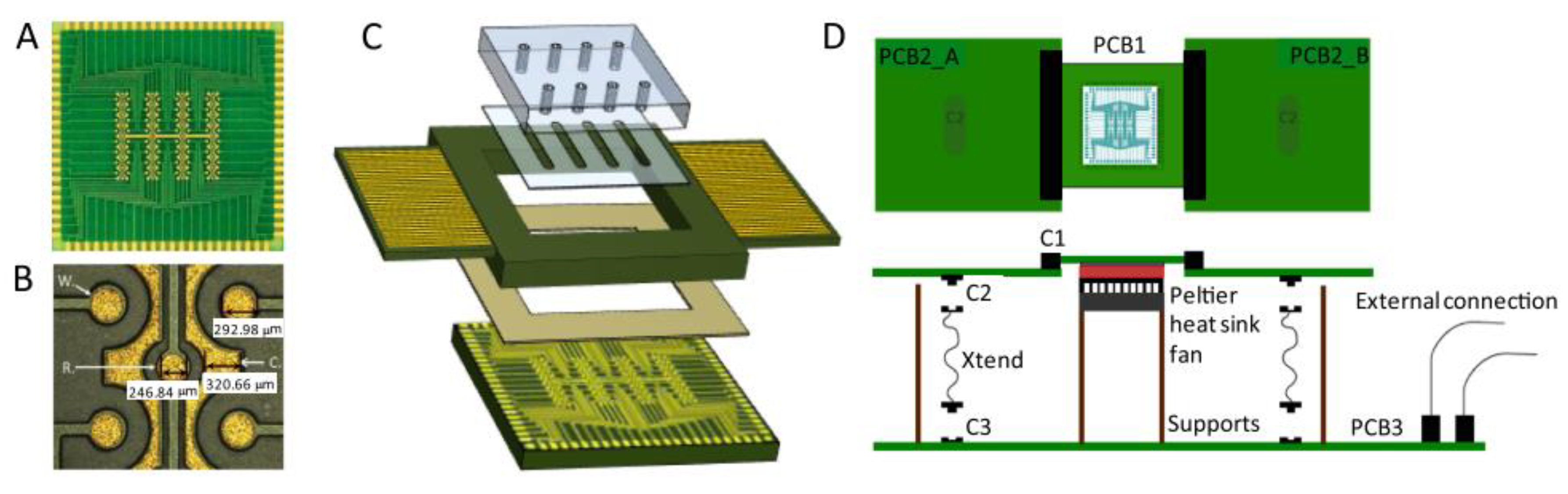


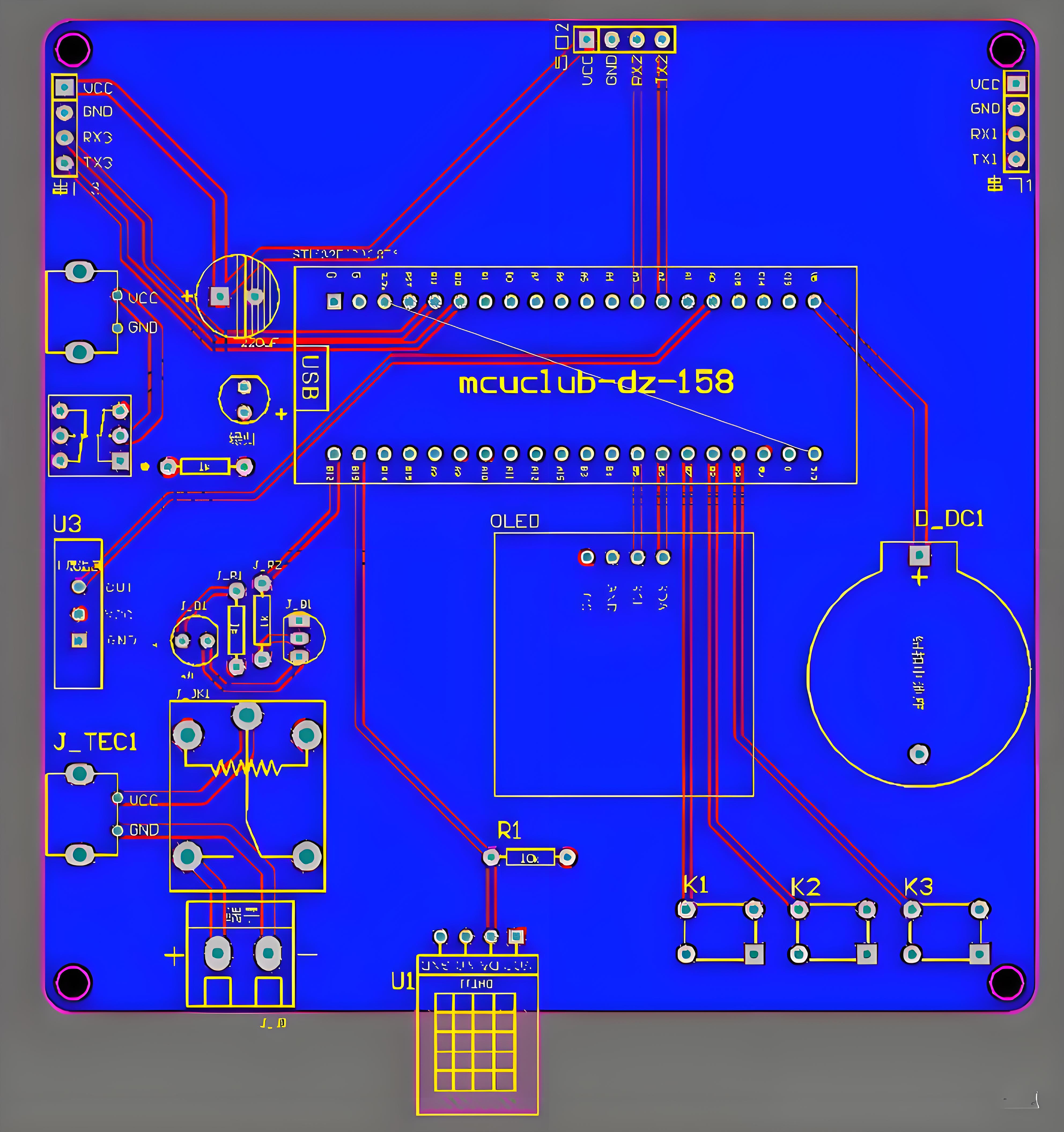
![30 Sensor interface PCB (Adapted from [77]) | Download Scientific Diagram](https://www.researchgate.net/publication/307138454/figure/fig27/AS:399958097317889@1472368849099/Sensor-interface-PCB-Adapted-from-77.png)


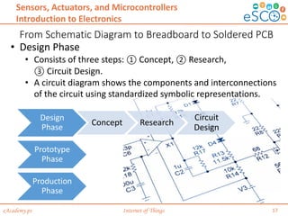
![Experimental Sensor design on a PCB developed in [35]. | Download ...](https://www.researchgate.net/publication/348776836/figure/fig7/AS:1010644895682562@1617967928555/Experimental-Sensor-design-on-a-PCB-developed-in-35.png)


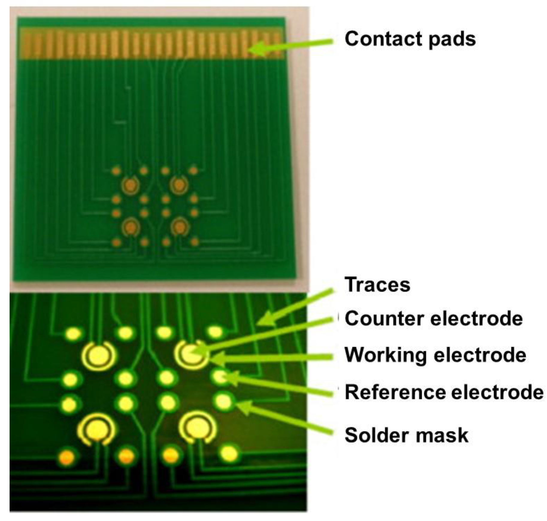


Plan adventures with our travel sensor interface board and pcb design | download scientific diagram gallery of substantial collections of inspiring images. exploratively showcasing artistic, creative, and painting. designed to inspire wanderlust and exploration. Our sensor interface board and pcb design | download scientific diagram collection features high-quality images with excellent detail and clarity. Suitable for various applications including web design, social media, personal projects, and digital content creation All sensor interface board and pcb design | download scientific diagram images are available in high resolution with professional-grade quality, optimized for both digital and print applications, and include comprehensive metadata for easy organization and usage. Our sensor interface board and pcb design | download scientific diagram gallery offers diverse visual resources to bring your ideas to life. Cost-effective licensing makes professional sensor interface board and pcb design | download scientific diagram photography accessible to all budgets. Multiple resolution options ensure optimal performance across different platforms and applications. Instant download capabilities enable immediate access to chosen sensor interface board and pcb design | download scientific diagram images. The sensor interface board and pcb design | download scientific diagram archive serves professionals, educators, and creatives across diverse industries. Time-saving browsing features help users locate ideal sensor interface board and pcb design | download scientific diagram images quickly.