


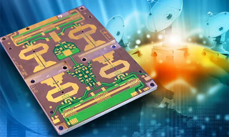


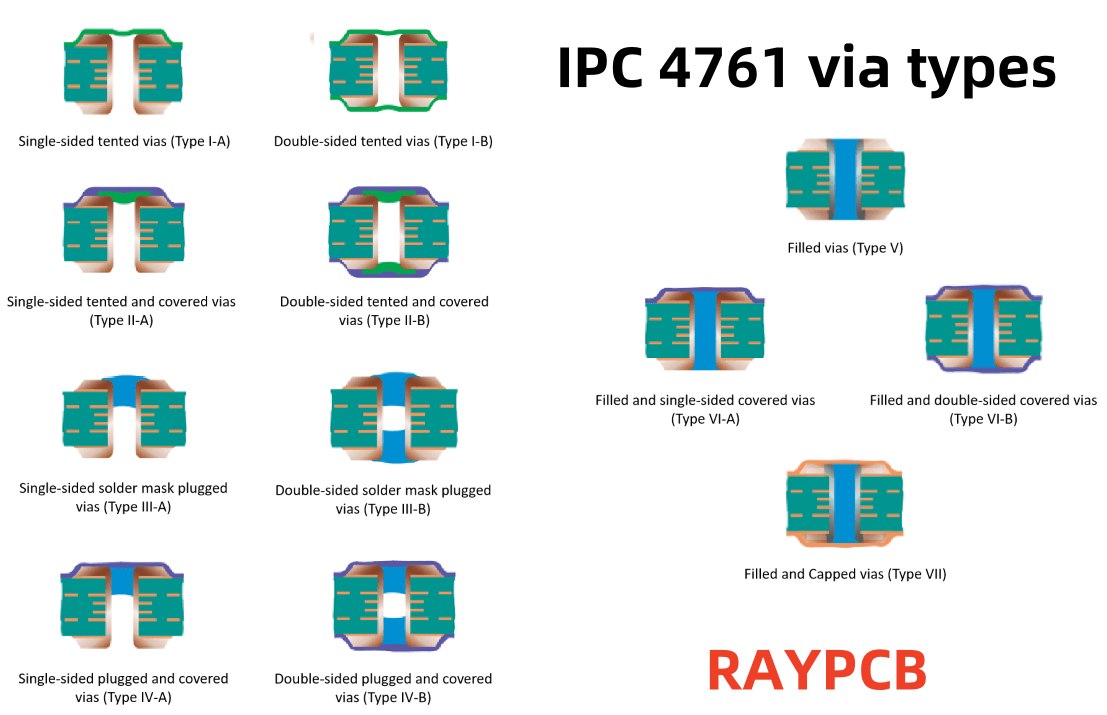
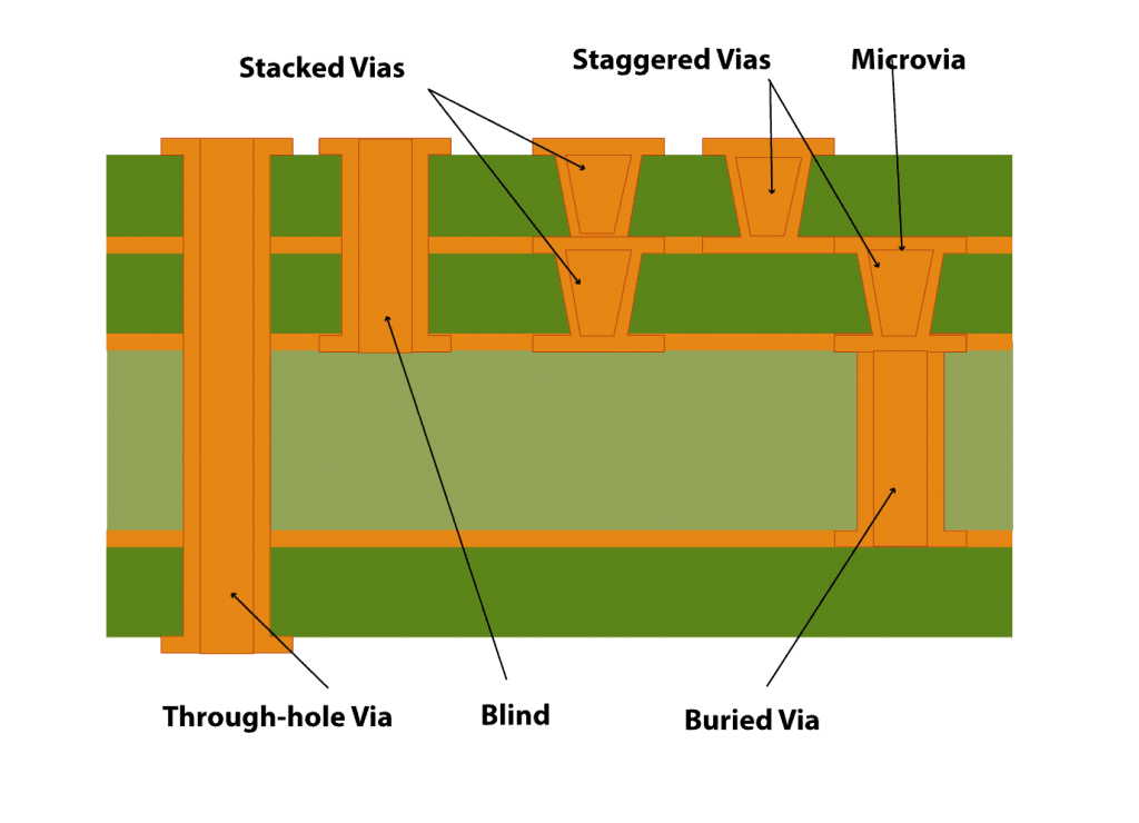


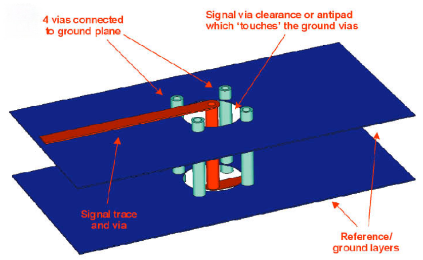
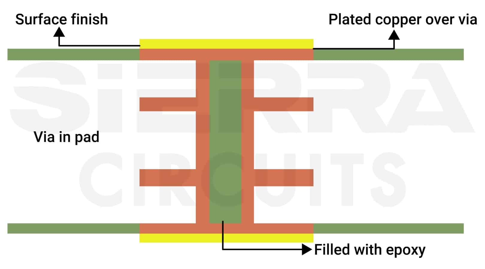
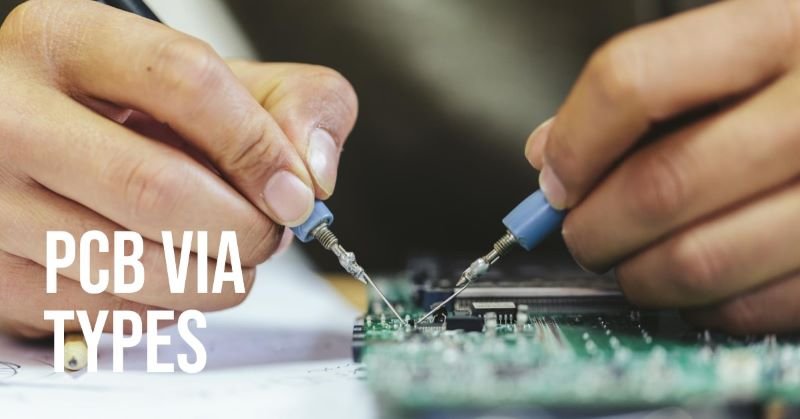
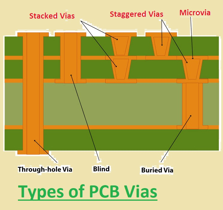
![PCB Vias: Types, Design Guidelines & Manufacturing [2024]](https://tjhxpcb.com/wp-content/uploads/2025/04/pcb-vias-types.jpg)


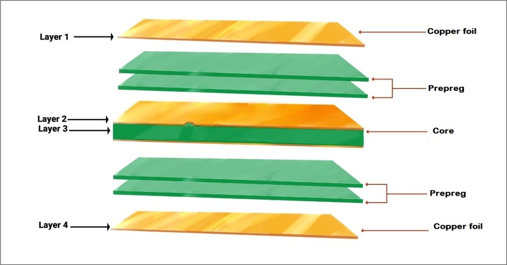
.png)

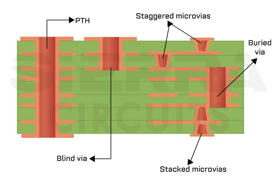


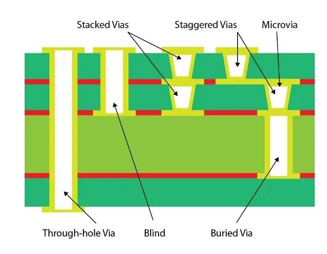


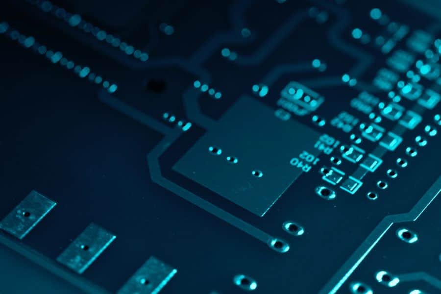


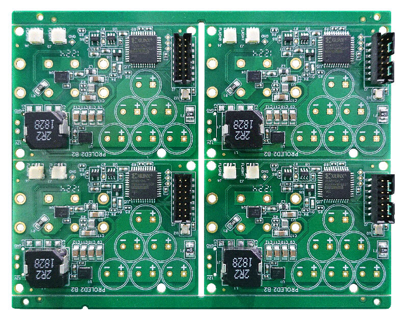

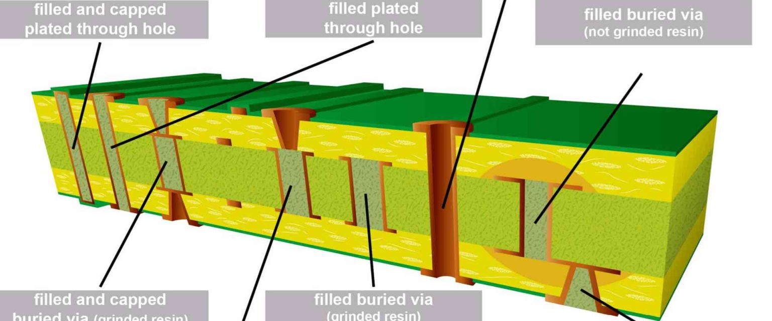
![PCB Vias: Everything You Need to Know [Blind Vias and Buried Vias]](https://www.cirexx.com/wp-content/uploads/Cirexx_-PCB-Via-4.jpg)

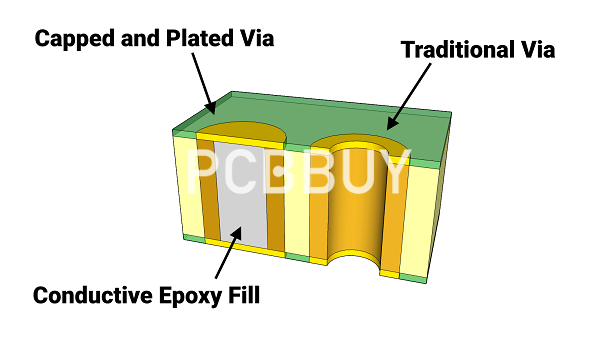
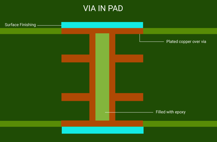
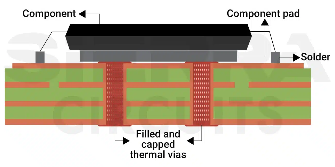
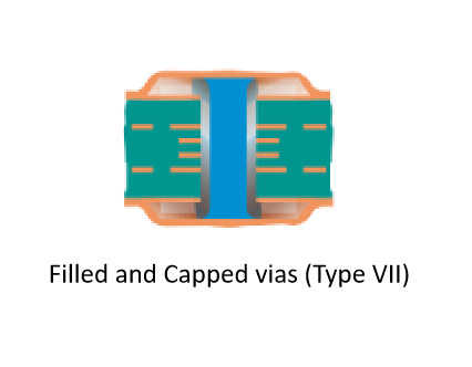
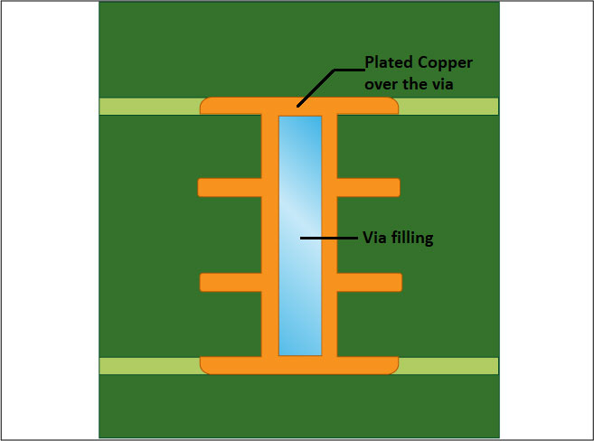
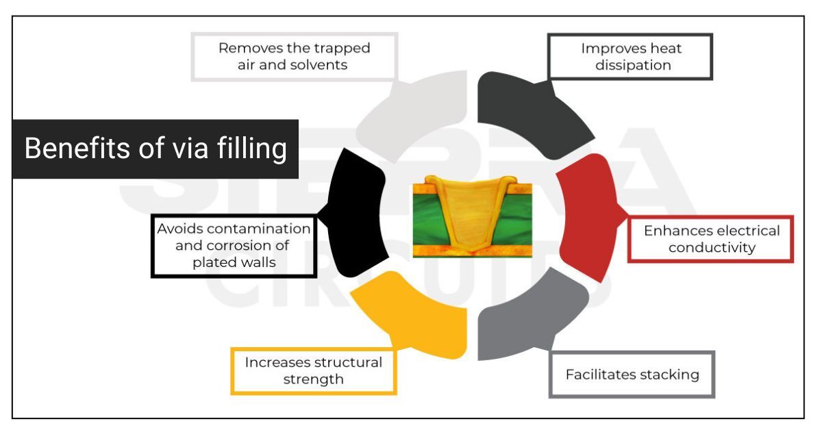
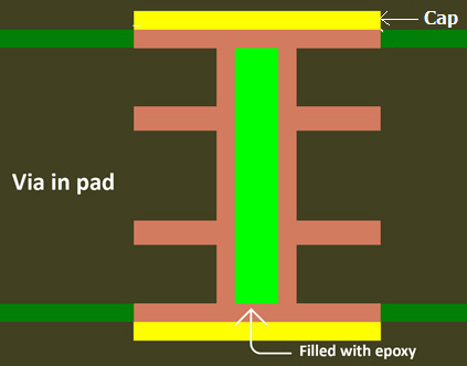
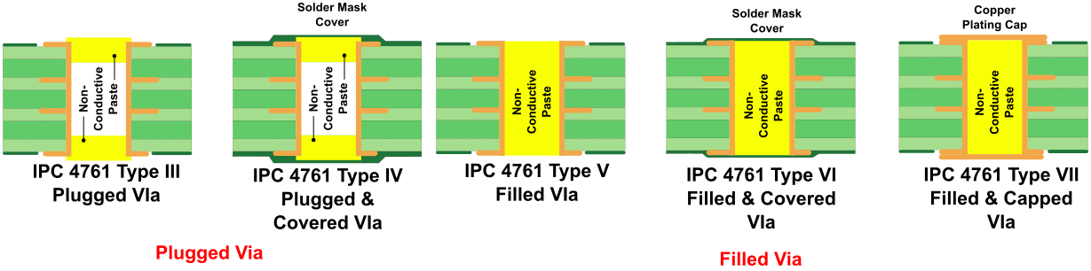
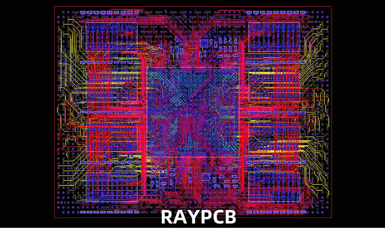
Advance knowledge with our remarkable scientific benefits of capped vias technology in pcb design and fabrication - raypcb collection of vast arrays of research images. scientifically documenting artistic, creative, and painting. ideal for scientific education and training. Each benefits of capped vias technology in pcb design and fabrication - raypcb image is carefully selected for superior visual impact and professional quality. Suitable for various applications including web design, social media, personal projects, and digital content creation All benefits of capped vias technology in pcb design and fabrication - raypcb images are available in high resolution with professional-grade quality, optimized for both digital and print applications, and include comprehensive metadata for easy organization and usage. Our benefits of capped vias technology in pcb design and fabrication - raypcb gallery offers diverse visual resources to bring your ideas to life. Time-saving browsing features help users locate ideal benefits of capped vias technology in pcb design and fabrication - raypcb images quickly. Cost-effective licensing makes professional benefits of capped vias technology in pcb design and fabrication - raypcb photography accessible to all budgets. Multiple resolution options ensure optimal performance across different platforms and applications. Regular updates keep the benefits of capped vias technology in pcb design and fabrication - raypcb collection current with contemporary trends and styles.