Please enter url.
Login
Logout
Please enter url.
Transmitter hardware configuration showing optical and RF power levels ...
researchgate.net
source
Comments
Figure 1 from External Cavity Laser for Chip-Scale Atomic Clock ...
Block diagram of the S-parameter test-set IC. | Download Scientific Diagram
Schematic diagram of the internal calibration system. | Download ...
Simplified schematic of CISR | Download Scientific Diagram
Simplified block diagram of PSR/CXI front-end and downconverter stages ...
L-band bread board down converter 1580MHz1780MHz down to dc-250MHz ...
Sensors | Free Full-Text | Vehicle Localization Kalman Filtering for ...
Block diagram of the proposed DC/AC converter system. | Download ...
Schematic of the diversity system. | Download Scientific Diagram
The structure of IIC-MUD for overloaded multiuser MIMO OFDM system ...
MICROCHIP dsPIC33 Dual Watchdog Timer User Guide
Simplified block diagram for a multiple resonator MKID readout system ...
Figure 2 from Simulation and analysis of MIMO-OFDM system based on ...
Figure 1 from Single event effects testing of a PLL and LVDS in a ...
The front-end of the SSRS | Download Scientific Diagram
Figure 1 from Design of a Class-B Power Amplifier at 2.4 GHz with ...
BER Test using a Signal Generator
Block diagram of the digital acquisition module. | Download Scientific ...
Example of dual band detection architecture. | Download Scientific Diagram
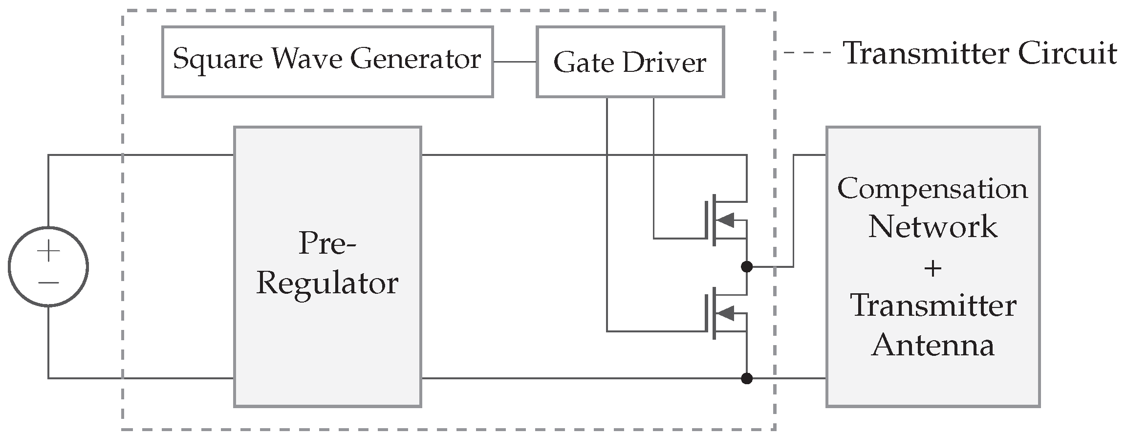
Sensors | Free Full-Text | Wireless Power Transfer: Systems, Circuits ...
TAM memory expansion for basic system with fixed access patterns ...
Block diagram of SDR platform. | Download Scientific Diagram
Block diagram of a time-domain stability measurement system for the ...
Set-up for the 20-Gb/s OTDM drop and detect experiment (PC-polarization ...
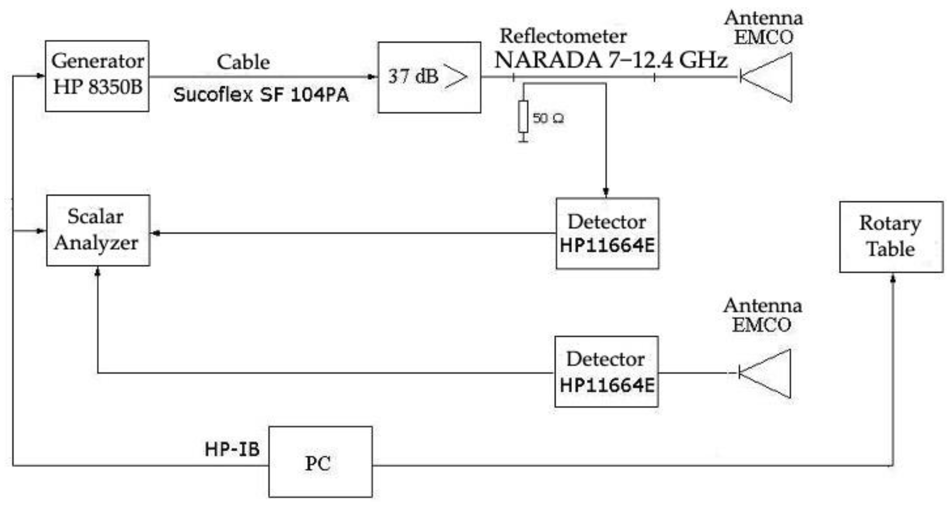
Hardware configuration for PCV test of the dipole array. | Download ...
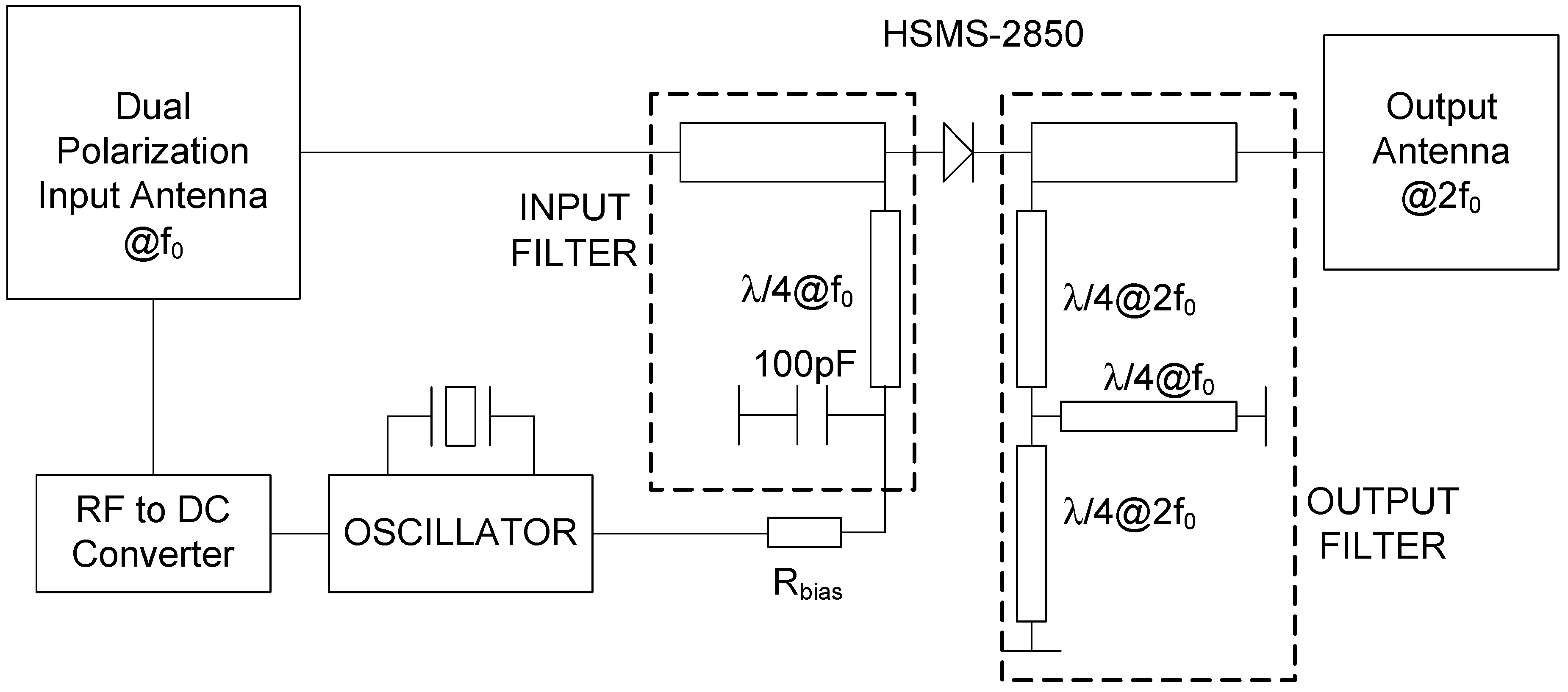
Sensors | Free Full-Text | Passive Harmonic RFID System for Buried ...
Remote Sensing | Free Full-Text | Quality Analysis of Small Maritime ...
RF System Block Diagram | Download Scientific Diagram
The hardware design of CSMA/CN | Download Scientific Diagram
Two layered reactive power control. | Download Scientific Diagram
Simulation model of the communication system. | Download Scientific Diagram
The quantum ampere is more precise than the conventional ampere - PTB.de
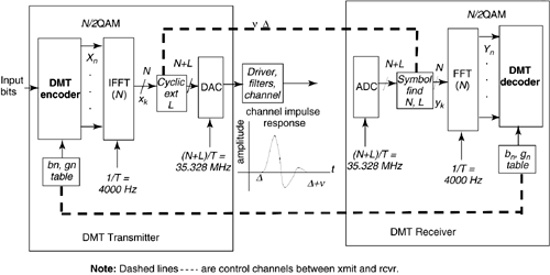
7.3 DMT Physical Layer Standard | DSL Advances
14: Real-Time FPGA Transmitter Block Diagram. PLL -Phase Locked Loop ...