Please enter url.
Login
Logout
Please enter url.
Engenharia de nanoestruturas de superfície. - [PDF Document]
documents.pub
source
Comments
Figure 1 from Comprehensive device reliability and oxide traps ...
Schematic illustration of the overall two-fold microfluidic process: a ...
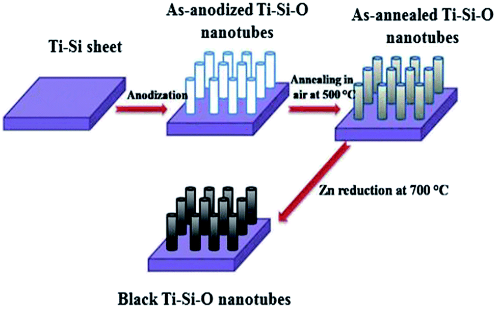
Black Si-doped TiO 2 nanotube photoanode for high-efficiency ...
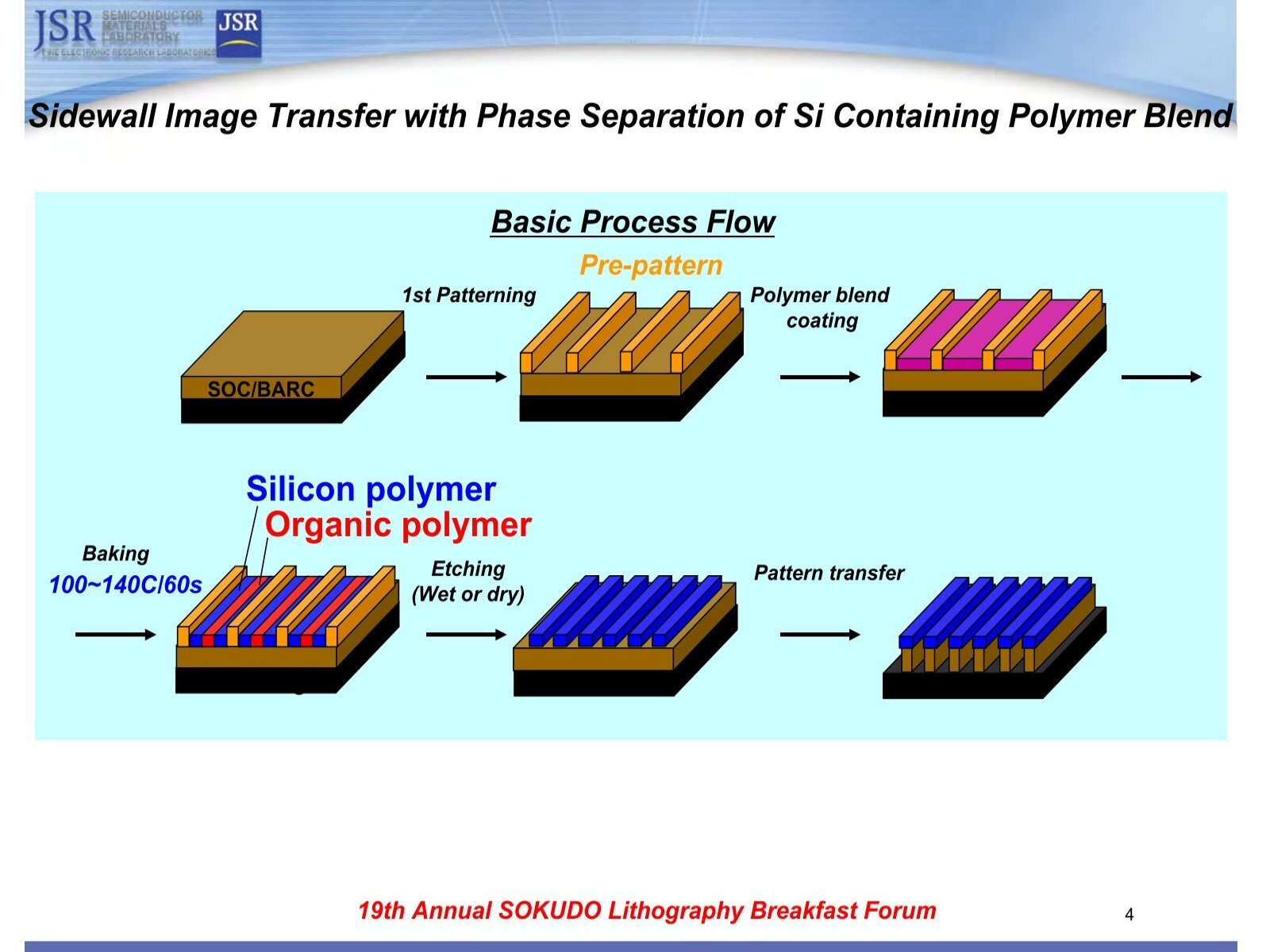
Sidewall Image Transfer w
Best Essay Writers Here - cvd graphene thesis - turnerthesis.web.fc2.com
Figure 11 from Extreme ultraviolet resist materials for sub-7 nm ...
Schematic illustration of fabrication process (a) Si and Mg ions are ...
Complete process flow of SU‐8 2050 photoresist electroplating mould ...
Figure 4 from A Review on Recent Advances in Transient Liquid Phase ...
Flexible Single-Crystalline Ge p-Channel Thin-Film Transistors With ...
(a) Schematic diagram of DMTD functionalized AlGaN/GaN HEMT for Pb 2 ...
2D advances to take center stage at IEDM – Tech Design Forum
Plasmonic Anti-Reflection Layer - F4News
WUBIN BAI | PhD | Northwestern University, IL | NU | Department of ...
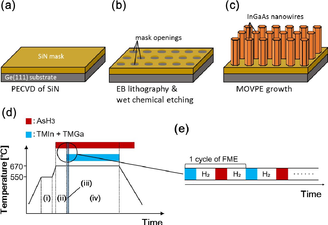
Figure 1 from Growth of InGaAs nanowires on Ge(111) by selective-area ...
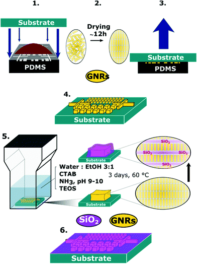
Hierarchical organization and molecular diffusion in gold nanorod ...
The process flow of the fabrication of a Dye-Sensitized Solar-Cell with ...
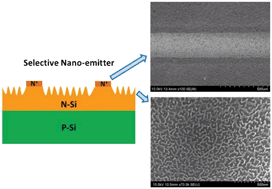
Selective nano-emitter fabricated by silver assisted chemical etch-back ...
Figure 1 from Tunable n-Type Doping of Carbon Nanotubes through ...
Attaining a significant improvement in battery life through the use of ...
Schematic diagram of fabricated p-Cu2O-shell/n-TiO2-nanowire-core for ...
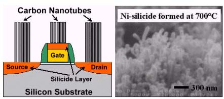
Schematic of the substrate for growing CNT and a cm square substrate on ...
(PDF) Metallization Method for Interdigitated Back-Contact Silicon ...
Fujitsu Is First to Achieve Vertical Growth and Diameter Control of ...
Brewer Science’s High-Temperature-Stable, Gapfilling Planarizing ...
Schematic diagram of the fabrication process of the graphene-based ...
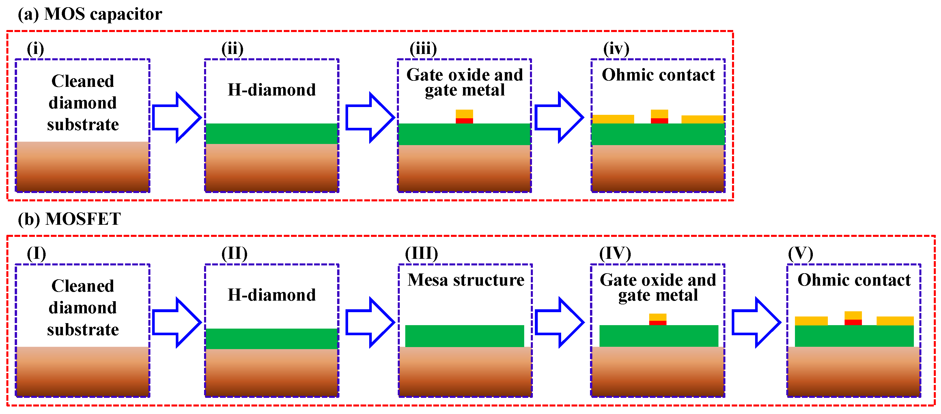
Sensors | Free Full-Text | An Overview of High-k Oxides on Hydrogenated ...
Schematic of the CVD reactor. | Download Scientific Diagram
FMR Measurements of Magnetic Nanostructures | IntechOpen
(a) Trace-gap and triple point (TP) in a power module building block ...
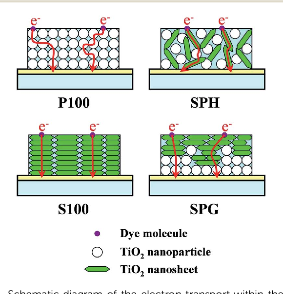
Figure 9 from Design of a TiO2 nanosheet/nanoparticle gradient film ...
CERN Has A LENR Colloquium
Schematic diagram of a Al/GO/ITO/PET (D1) and b Al/GO/HfOx/ITO/PET (D2 ...
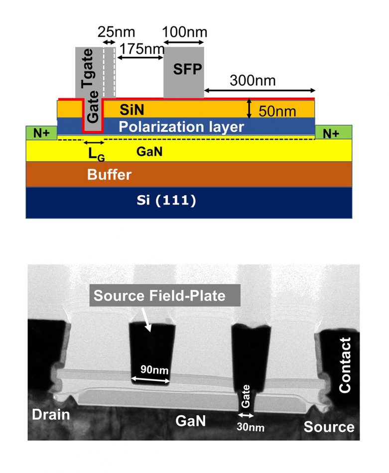
(PDF) Au-Free AlGaN/GaN Power Diode on 8-in Si Substrate With Gated ...
Schematic diagram of the solid phase reaction process to synthesize ...