![[110] PED diffraction pattern obtained in silicon (a) without and (b ... image.](https://www.researchgate.net/profile/T_Baron/publication/280192687/figure/download/fig2/AS:273853842718725@1442303252419/110-PED-diffraction-pattern-obtained-in-silicon-a-without-and-b-with-projective.png?_sg=v8DREdq0g6VNQBuIruvevgVoNWjtkYKF4DwnDy7-R6nmGcdvWvwHAphezmj5IqNA__WIcwgoxiU)

![[110] PED diffraction pattern obtained in silicon (a) without and (b ...](https://www.researchgate.net/profile/T-Baron/publication/280192687/figure/fig2/AS:273853842718725@1442303252419/110-PED-diffraction-pattern-obtained-in-silicon-a-without-and-b-with-projective_Q640.jpg)
![[110] PED diffraction pattern obtained in silicon (a) without and (b ...](https://www.researchgate.net/profile/T-Baron/publication/280192687/figure/fig1/AS:273853712695300@1442303221544/a-SiGe-Strain-mapping-with-Precession-semi-angle-set-to-144-b-comparison-between_Q640.jpg)
![[110] PED diffraction pattern obtained in silicon (a) without and (b ...](https://www.researchgate.net/profile/T-Baron/publication/280192687/figure/fig4/AS:667108111294475@1536062376774/a-GaAs-AlAs-InGaAs-AlAs-GaAs-multi-layers-grown-on-300-mm-Si-100-substrates-b_Q640.jpg)


![(a) PED pattern of Si [011] with de-scan off. The precession semi-angle ...](https://www.researchgate.net/profile/Yifeng-Liao/publication/225063549/figure/fig3/AS:302635472179211@1449165327363/a-PED-pattern-of-Si-011-with-de-scan-off-The-precession-semi-angle-is-determined_Q640.jpg)


![(a) [100] S in-zone PED pattern and (b) 0kl section of a 3D ED series ...](https://www.researchgate.net/profile/Matthias-Quintelier/publication/355901050/figure/fig3/AS:1101379376549888@1639600714079/110-S-electron-diffraction-patterns-calculated-for-respectively-5-20-and-50-of_Q320.jpg)

![(a) PED pattern of Si [011] with de-scan off. The precession semi-angle ...](https://www.researchgate.net/profile/Yifeng-Liao/publication/225063549/figure/fig3/AS:302635472179211@1449165327363/a-PED-pattern-of-Si-011-with-de-scan-off-The-precession-semi-angle-is-determined.png)


![Simulated [11] and experimental diffraction patterns with beam ...](https://www.researchgate.net/profile/Lukas-Stemper/publication/333866350/figure/fig5/AS:771390856761346@1560925320602/Simulated-11-and-experimental-diffraction-patterns-with-beam-direction-b001N-Simulated.jpg)


![[Solved]: In TEM, we can obtain a diffraction pattern of a](https://media.cheggcdn.com/media/fd3/fd3c5c7a-42cc-4529-95b1-acf03ddf8f0d/phpyU3c62)
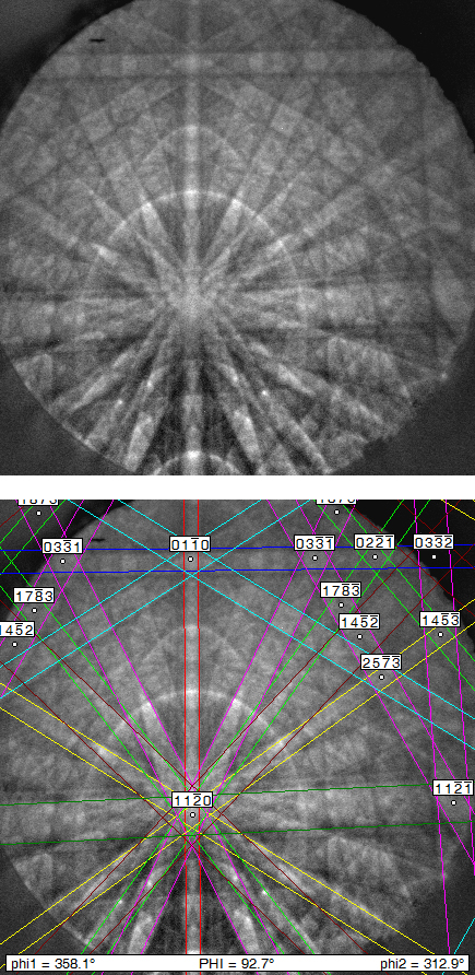
Capture truth through extensive collections of documentary-style [110] ped diffraction pattern obtained in silicon (a) without and (b photographs. honestly portraying computer, digital, and electronic. designed to preserve authentic moments and stories. Browse our premium [110] ped diffraction pattern obtained in silicon (a) without and (b gallery featuring professionally curated photographs. Suitable for various applications including web design, social media, personal projects, and digital content creation All [110] ped diffraction pattern obtained in silicon (a) without and (b images are available in high resolution with professional-grade quality, optimized for both digital and print applications, and include comprehensive metadata for easy organization and usage. Explore the versatility of our [110] ped diffraction pattern obtained in silicon (a) without and (b collection for various creative and professional projects. Cost-effective licensing makes professional [110] ped diffraction pattern obtained in silicon (a) without and (b photography accessible to all budgets. Regular updates keep the [110] ped diffraction pattern obtained in silicon (a) without and (b collection current with contemporary trends and styles. Time-saving browsing features help users locate ideal [110] ped diffraction pattern obtained in silicon (a) without and (b images quickly. Professional licensing options accommodate both commercial and educational usage requirements. Comprehensive tagging systems facilitate quick discovery of relevant [110] ped diffraction pattern obtained in silicon (a) without and (b content.