Please enter url.
Login
Logout
Please enter url.
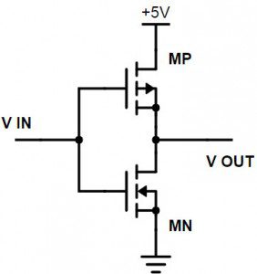
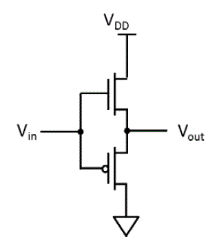
Cmos Transistor Symbol
animalia-life.club
source
Comments
CMOS Technology : Working Principle, Characteristics & Its Applications
Solved (10 points) Consider the CS amp with a | Chegg.com
Short-circuit current in CMOS inverter. | Download Scientific Diagram
Solved Consider the CS amp with a current source load. Vin = | Chegg.com
Solved at 10 kHz adjust Vin to obtain 150 mV peak-to-peak | Chegg.com
A.2.2.1 CMOS Inverters
CMOS Logic Inverter - Transfer Function
Solved An engineer has come up with a new design for a | Chegg.com
digital logic - XOR gate; transistor level design - Electrical ...
Basic Gate-Diffusion-Input cell [2]-[5] | Download Scientific Diagram
Solved Consider the following CMOS inverter shown in Figure | Chegg.com
Is it correct to claim that the logic circuits are only special using ...
Reverse engineering the popular 555 timer chip (CMOS version)
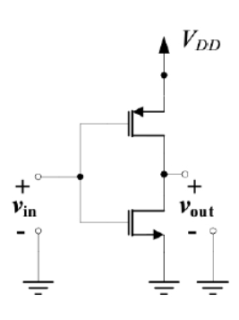
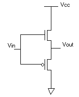
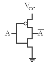
The structure of the CMOS inverter which contains two complementary ...
The AC model of the improved MOSFET-only circuit | Download Scientific ...
Solved The two figures given above show a CMOS inverter | Chegg.com
Bias-stabilized inverter-amplifier: an inspiring solution for low ...
Electronics hardware interview questions
Lab
Simple common source stage. | Download Scientific Diagram
The Current Starved Delay Element (CSDE) | Download Scientific Diagram
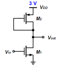
PMOS-Load-Inverter Analog-CMOS-Design || Electronics Tutorial
GitHub - AishikAnalogCKTdesign/DFF-using-2-1-MUX: DFF and 2:1 MUX are ...
ECE 109 - Test #1 Flashcards | Quizlet
NBTI’s impact on timing - EDN
Visualization of R-bar approach used for Monte Carlo simulations ...
Figure 11 from Design of Operational Transconductance Amplifier using ...
Garima Verma , Industrial Engineering Concepts: CMOS: NOT Gate Design ...
Commonly used voltage mode readout circuits: direct bias approach (a ...
(PDF) Design and Analysis of Super Source Follower
Schematic diagram for the skewed delay cell [3]. | Download Scientific ...
NOT Gate: The Building Block (Transistors to Tiny Circuits!)
FBB multimode multi-threshold CMOS technique. | Download Scientific Diagram
How do I compute \$V_{out}\$ in a MOSFET? - Electrical Engineering ...
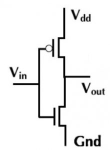
NOT Gate - Circuits - Circuit Diagram
BiCMOS-Inverter
CMOS-Inverter-Diagram
CMOS-Inverter-Truth-Table
Inverter-Using-CMOS
CMOS-Inverter-Schematic
Transistor-Inverter
Inverter-Circuit
CMOS-Inverter-Layout
5000W-Inverter-Circuit-Diagram
N-MOSFET-Inverter
Power-Inverter-Circuit-Diagram
Sine-Wave-Inverter-Circuit-Diagram
CMOS-Inverter-Cadence
CMOS-Inverter-Cross-Section
Pure-Sine-Wave-Inverter-Circuit-Diagram
Inverter-Stick-Diagram


![Schematic diagram for the skewed delay cell [3]. | Download Scientific ...](https://www.researchgate.net/publication/224647829/figure/fig3/AS:669008827252738@1536515542320/Schematic-diagram-for-the-skewed-delay-cell-3.png)