Please enter url.
Login
Logout
Please enter url.
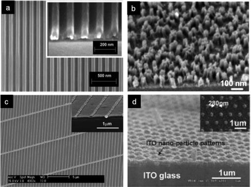
(a) Top view of RIE textured surface, (b) cross sectional view of RIE ...
researchgate.net
source
Comments
SEM images of a nanoisland laser. (a) The colored area describes the ...
(a) HAADF cross section image (a) and detail (b) of a Mn-deficient LSMy ...
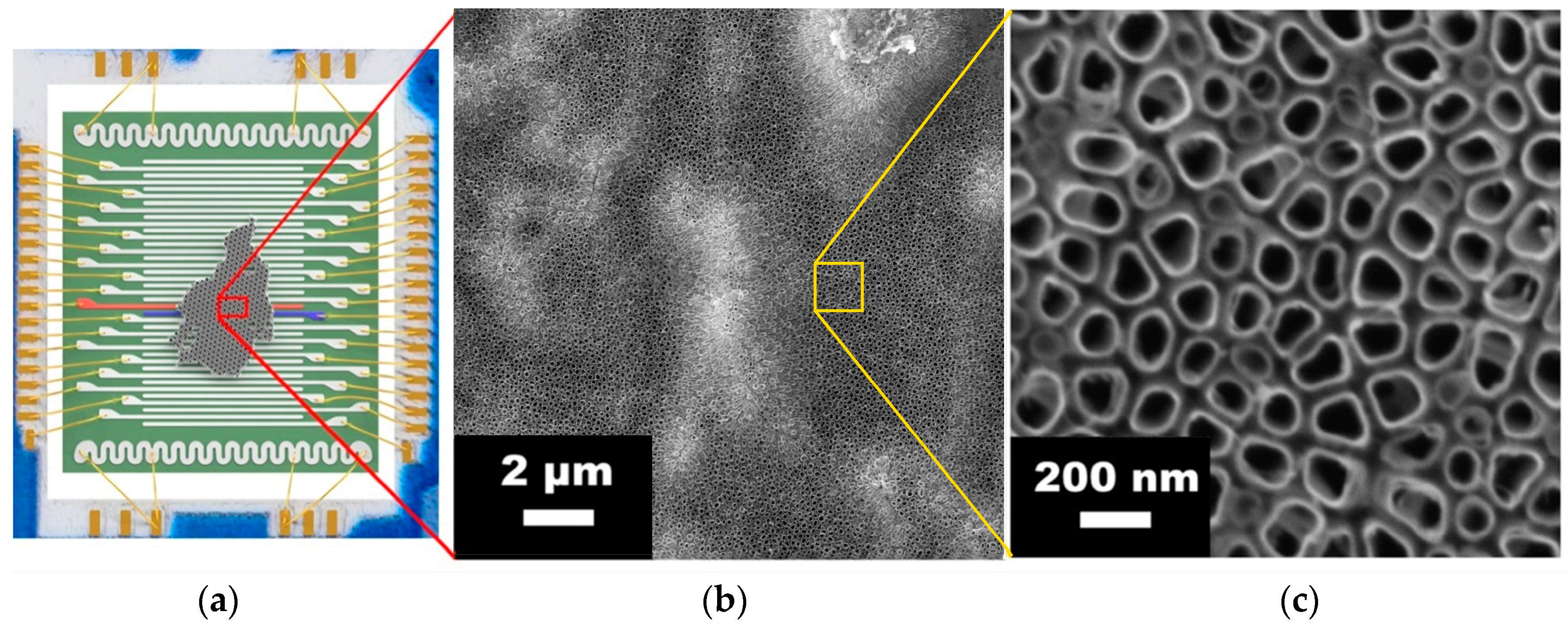
Displacement Talbot lithography for nano-engineering of III-nitride ...
Figure 1 from Selective Wet-Etching of Silicon Germanium in Composite ...
Nanomaterials | Free Full-Text | Light-Tuned DC Conductance of Anatase ...
3D-FDTD simulation and PC cavity a Fundamental TE mode band diagram of ...
Schematic and corresponding SEM characterization of the fabrication ...
SEM in-plane image of the fabricated 2D PhC membrane: the inset shows ...
(a) SEM images of the DFB grating imprinted into a MAPbBr 3 layer with ...
Materials | Free Full-Text | Development of Hybrid Surfaces with ...
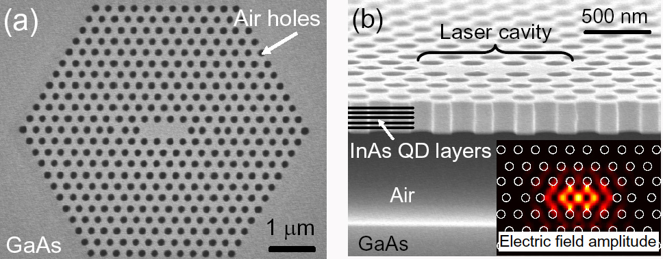
A photonic crystal nanocavity laser with ultralow threshold
(a) Scheme of DLD size sorting principle; (b) SEM picture of DLD ...
The state of nanoimprinted polymer organic solar cell technology
Nonlinear optics with resonant metasurfaces | MRS Bulletin | Cambridge Core
(a) SEM image showing the hexagonal design of the thermoelectric ...
TiO2 pillars on a silicon substrate. Pillar edge‐to‐edge spacing of ...
(PDF) Potential solutions for 193 nm lithography challenges at 45 and 32 nm
(Top) Schematic representation of pattern transfer from supramolecular ...
A) Electron microscopy images of the β-MnOOH nanostructures prepared ...
Nanoscale Printing System – Nano OPS
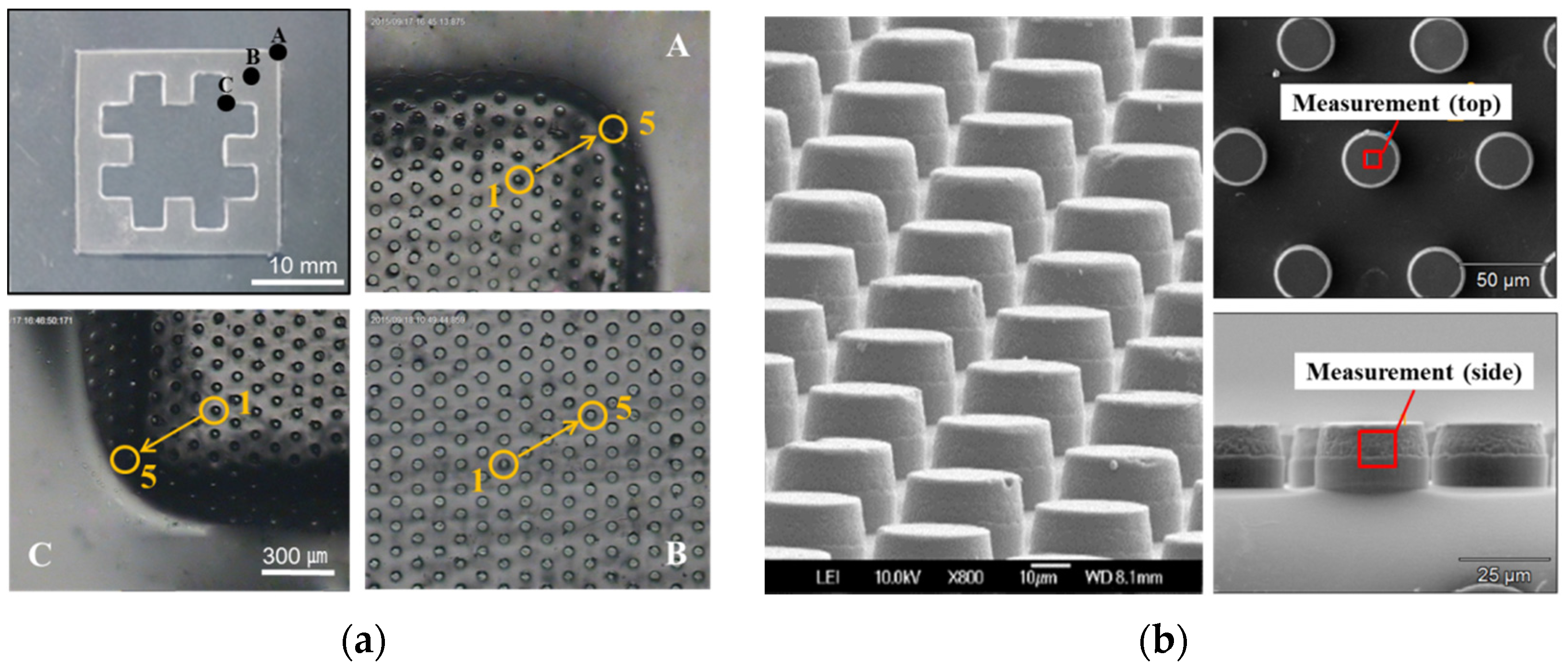
SEM micrograph of the device, the spacing between the micro-pillars in ...
Conventional and Un-Conventional Lithography for Fabricating Thin Film ...
(PDF) Microneedles for Transdermal Biosensing: Current Picture and ...
Terahertz in-line hologram of the steel blade of a screwdriver and its ...
REU: National Nanotechnology Coordinated Infrastructure | SRP | Nebraska
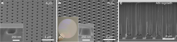
Synthesis and Characteristics of Transferrable Single‐Crystalline AlN ...
Figure 3 from Ongoing Evolution of DRAM Scaling via Third Dimension ...
Scanning Electron Microscopy (SEM) image of the micro-cavity structure ...
Disjointed hook metasurface (DHM). (A) Schematic of the DHM with the ...
Applied Sciences | Free Full-Text | A Review of X-ray Microcalorimeters ...
Micromachines | Free Full-Text | Bio-Inspired Wide-Angle Broad-Spectrum ...
The diagram and FIB image of the multilayer fishnet sample are ...
SEM image of bottom-up grown GaN nanostructures. (a) Self-organized GaN ...
(a) 30°-tilted SEM of as-grown GaAs nanowires on Si substrates with ...
0.1 | Preliminary results. (a) and (b) HAADF STEM image of ultra-low ...