Please enter url.
Login
Logout
Please enter url.
Szankció Gyorsítani Szieszta jk flip flop megvet Alcatrazsziget Gyártó ...
analiticaderetail.com
source
Comments
J-K Flip-Flop - Flip-Flops - Basics Electronics
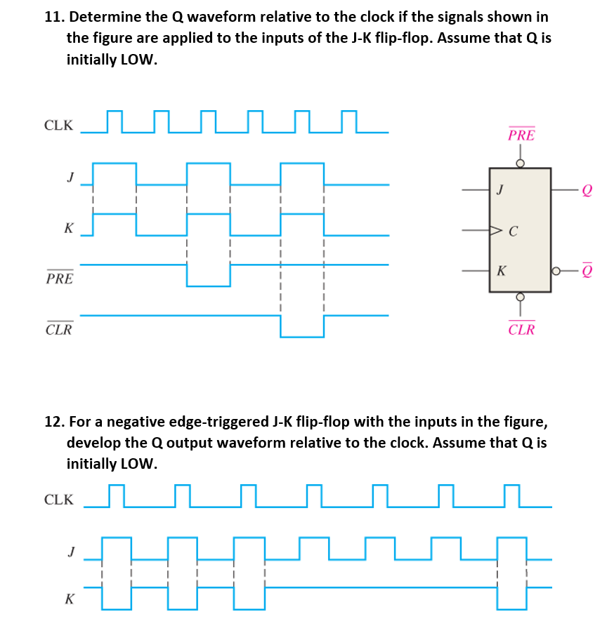
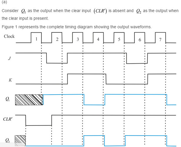
Solved 11. Determine the Q waveform relative to the clock if | Chegg.com
(Solved) - For the following JK flip flops, complete each of the timing ...
Nonlinear Control of an Induction Machine using Robust Controller based ...
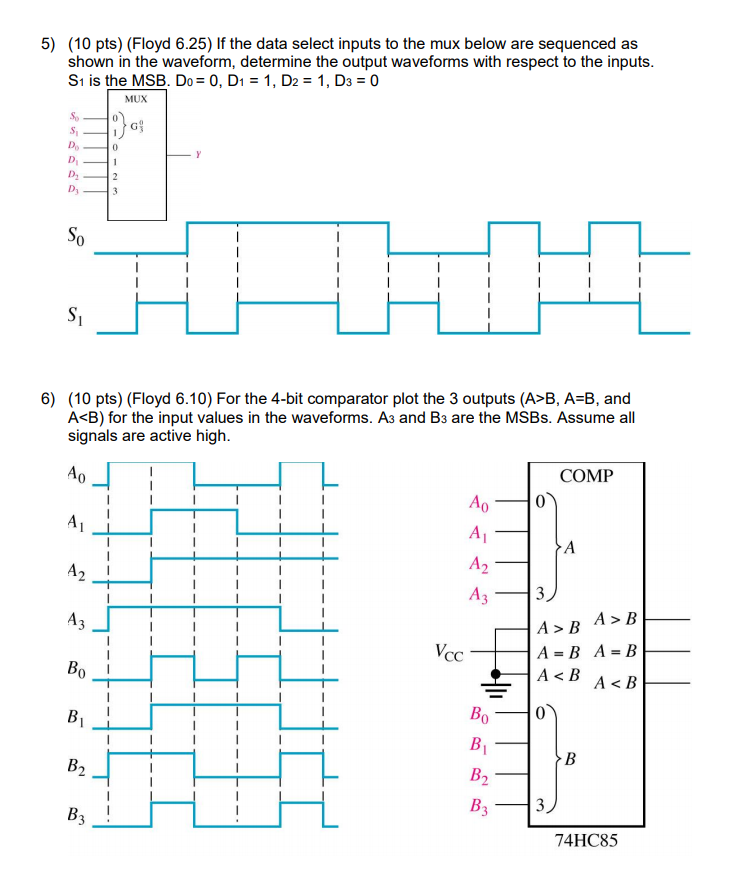
Solved 5) (10 pts) (Floyd 6.25) If the data select inputs to | Chegg.com
Ring Counter - Counters - Basics Electronics
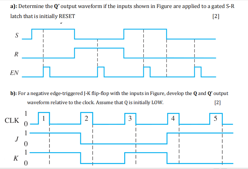
Solved a): Determine the Q'output waveform if the inputs | Chegg.com
Solved Question 7 [18 MARKS - (a) 1 mark, (b) 5 marks, (c) 6 | Chegg.com
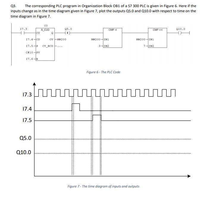
Q3. The corresponding PLC program in Organization | Chegg.com
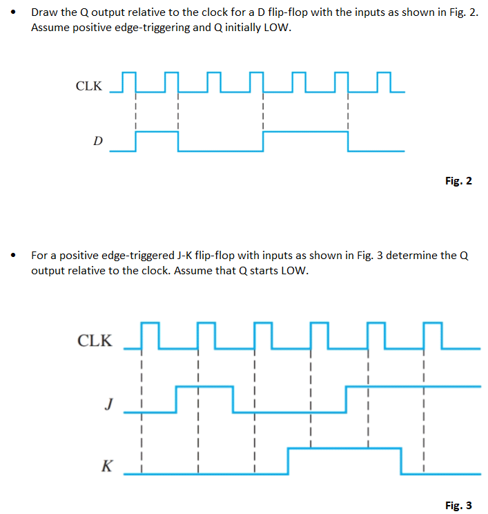
Solved: Draw the Q output relative to the clock for a D fl
[Solved] 1. If the S and A waveforms in figure la are applied to the ...
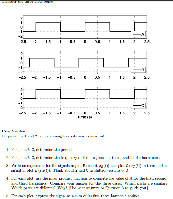
Solved Consider the three plots below: Do problems 1 and 2 | Chegg.com
Figure 4 from A Glitch Key-Gate for Logic Locking | Semantic Scholar
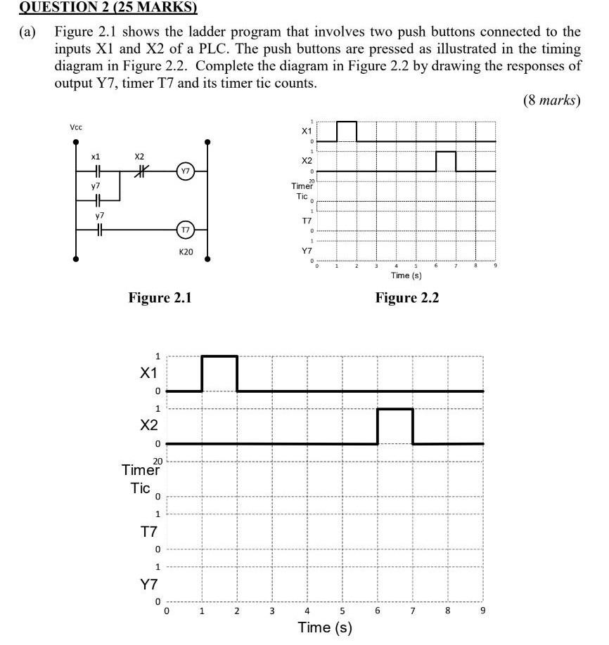
Solved a) Figure 2.1 shows the ladder program that involves | Chegg.com
Solved How did they get this truth table for the JK flip | Chegg.com
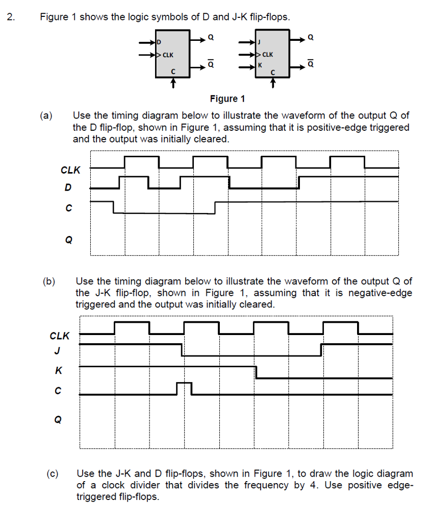
Solved Figure 1 shows the logic symbols of D and J-K | Chegg.com
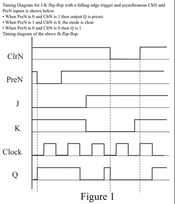
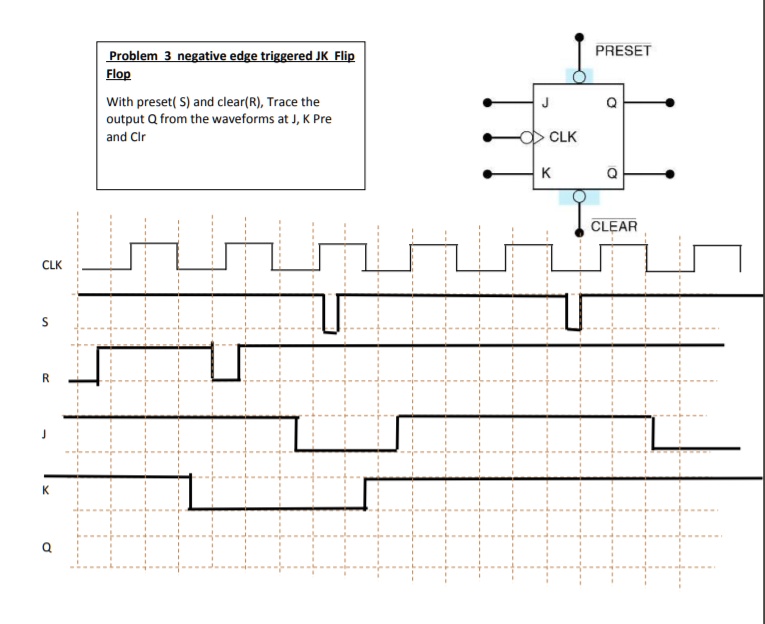
SOLVED: Problem 3: Negative Edge-Triggered JK Flip Flop PRESET With ...
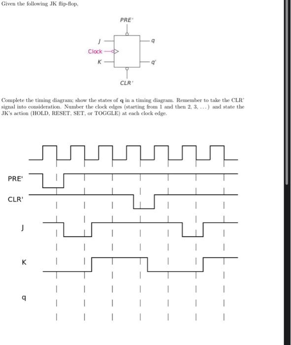
Given the following JK flip-flop, Complete the timing | Chegg.com
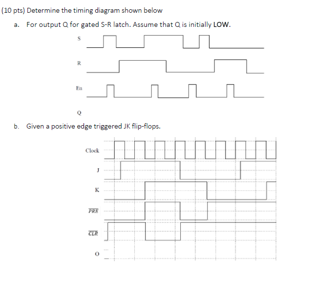
Solved (10 pts) Determine the timing diagram shown below a. | Chegg.com
CCNA Exploration 1: Introduction to Networks: Encoding & Signaling ...
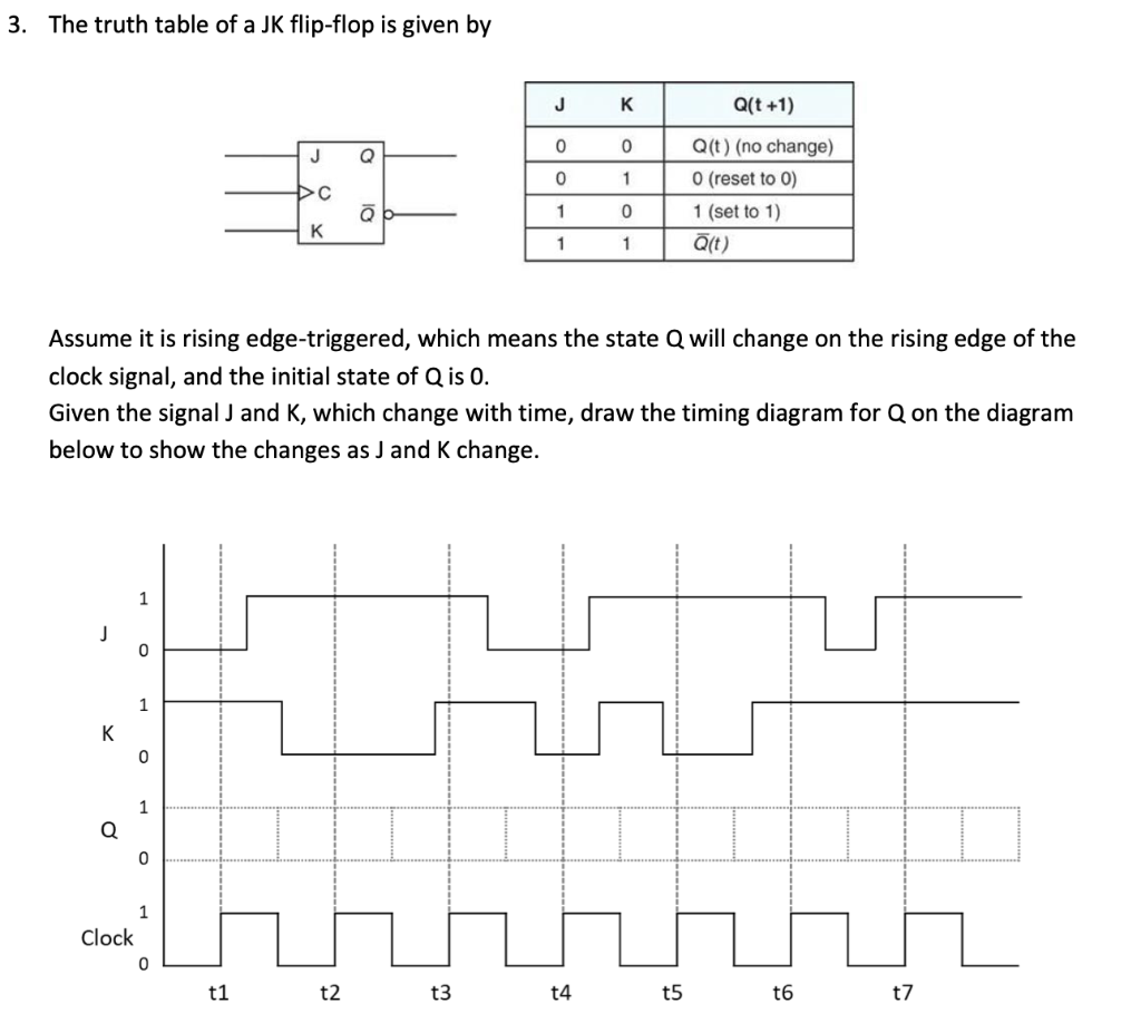
Solved Computer Architecture Question: Given the signal J | Chegg.com
Solved Q1 change state on rising edge of clock pulse(=value | Chegg.com
Output pulses for counter clockwise (CCW) and clockwise direction of ...
The following figure shows a logic gate circuit with two inputs A and B ...
Timing diagram example for the internal nodes of 74LS74 D-FF [6] Fig.6 ...
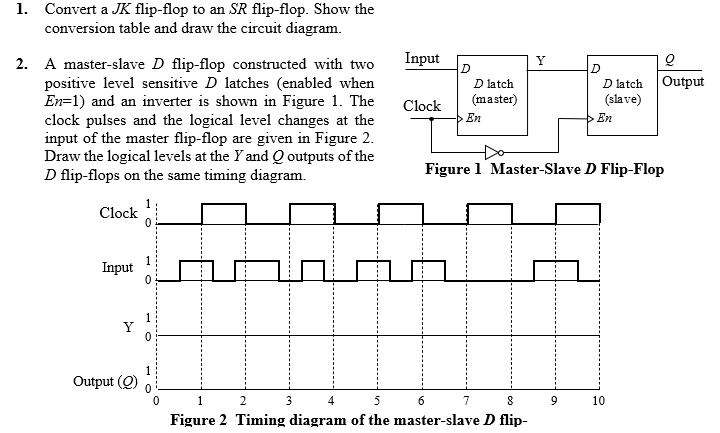
Solved 1. Convert a JK flip-flop to an SR flip-flop. Show | Chegg.com
Solved Complete the timing diagrams for the points shown in | Chegg.com
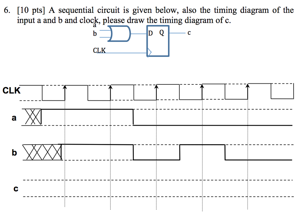
Solved A sequential circuit is given below, also the timing | Chegg.com
Solved 4) The input signals below are applied to the | Chegg.com
Schematic of chirp-managed laser as DPSK transmitter. | Download ...
Solved Please solve showing how to do it, do not use other | Chegg.com
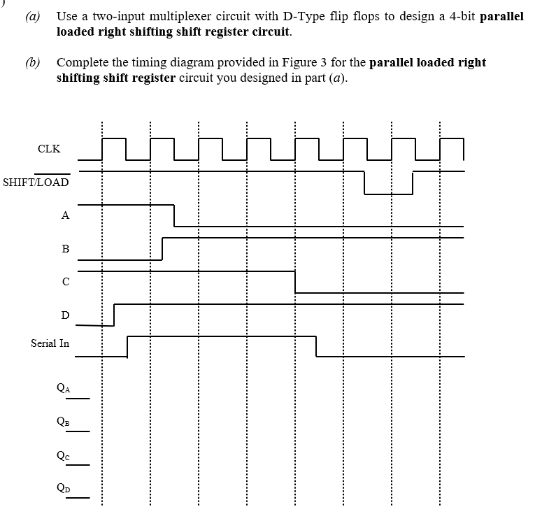
Solved (a) Use a two-input multiplexer circuit with D-Type | Chegg.com
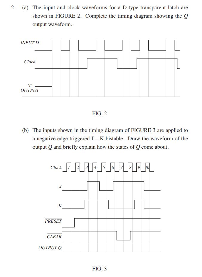
Solved (a) The input and clock waveforms for a D-type | Chegg.com
What is a positive edge triggered flip flop - vvtiplum
(a) Complete the following timing diagram for a J-K | Chegg.com
Sr-Flip-Flop
RS-Flip-Flop
Jk-Flip-Flop-Diagram
Flip-Flop-Circuit
Jk-Flip-Flop-Table
T-Flip-Flop
Sr-Flip-Flop-Truth-Table
Flip-Flop-Logic-Diagram
Flip-Flop-Types
Clocked-Jk-Flip-Flop
Jk-Flip-Flop-Schematic
Jk-Latch
D-Flip-Flop
Jk-Flip-Flop-with-Clear
D-Flip-Flop-Timing-Diagram
Jk-Flip-Flop-Using-CMOS


![Timing diagram example for the internal nodes of 74LS74 D-FF [6] Fig.6 ...](https://mavink.com/images/loadingwhitetransparent.gif)