


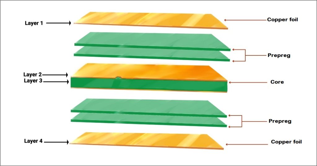
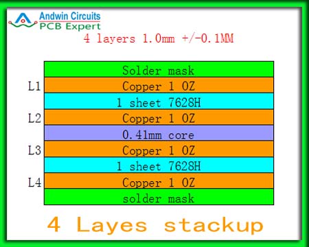


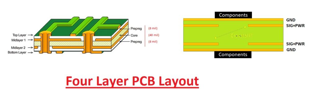
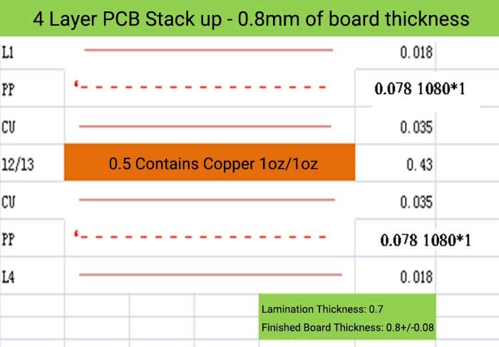
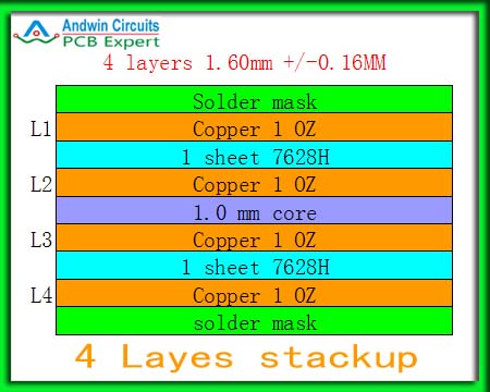


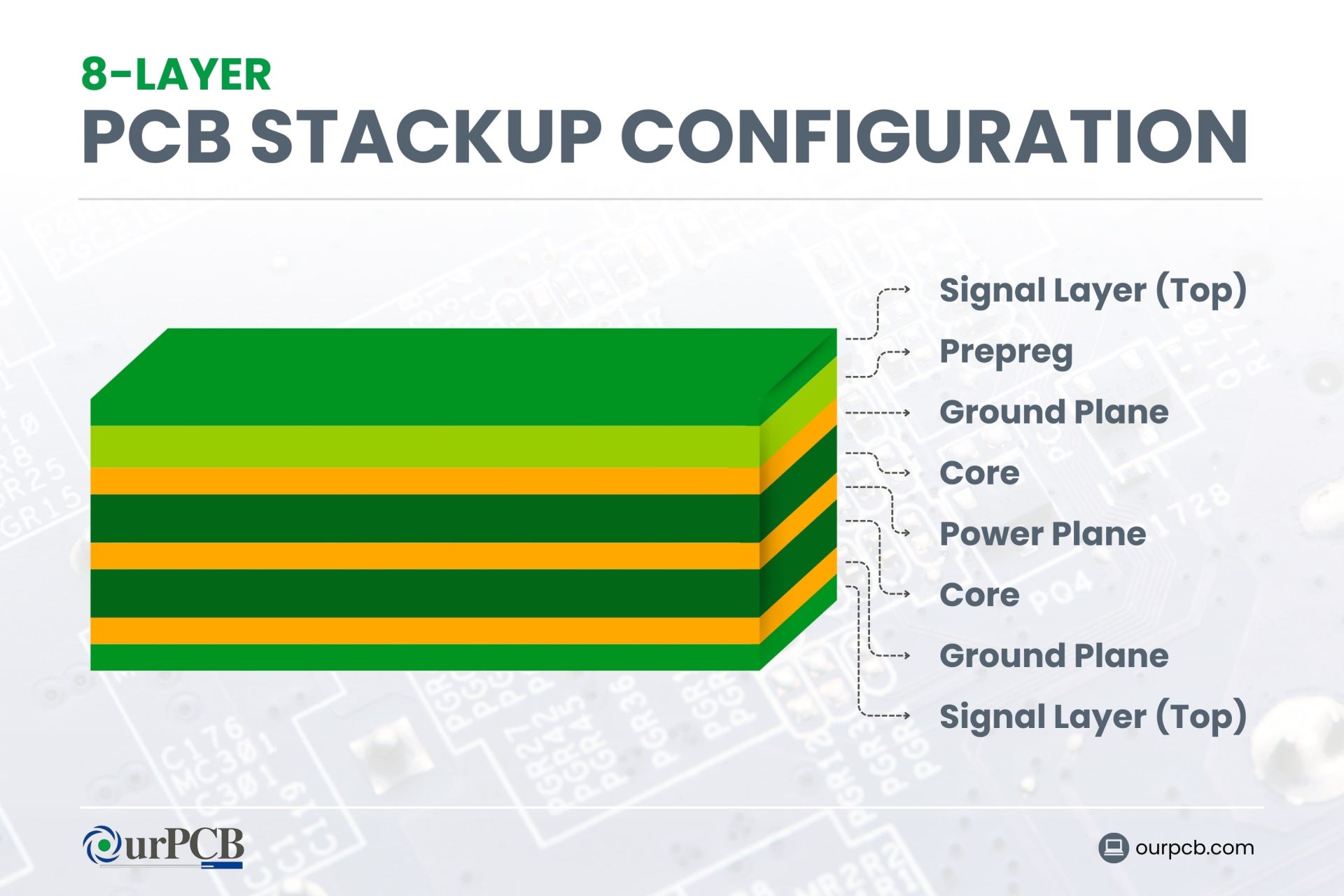


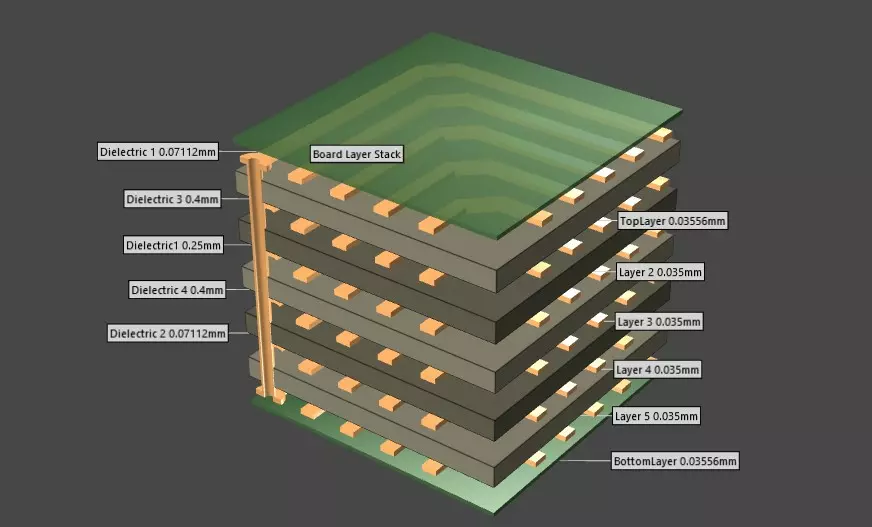
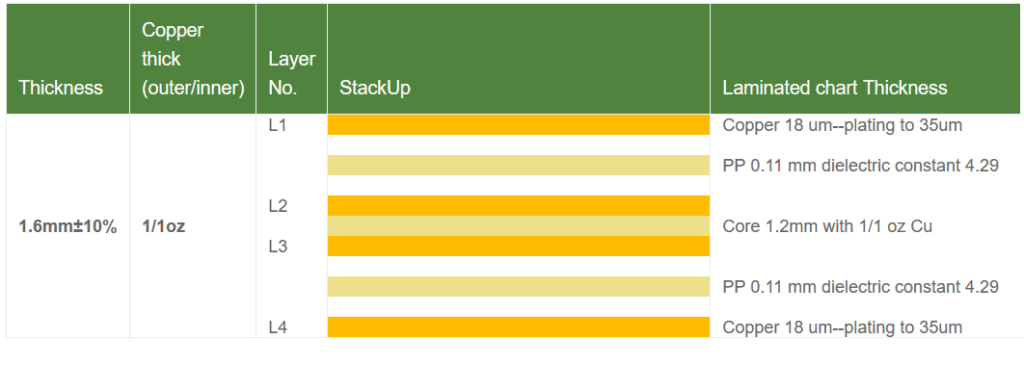
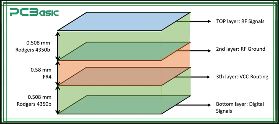


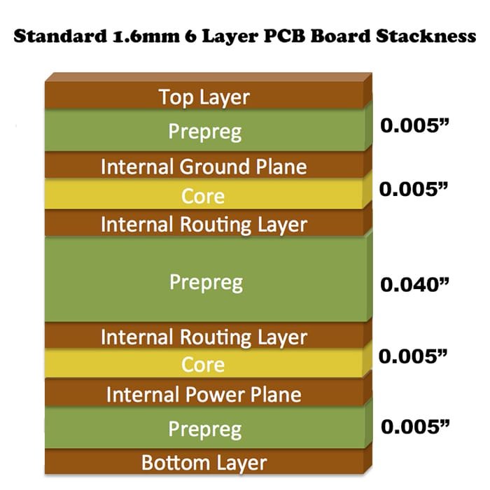


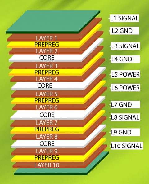


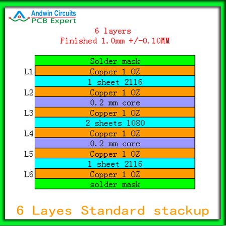
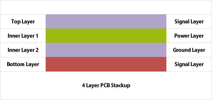
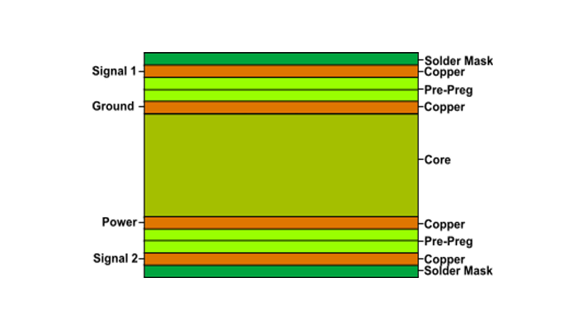


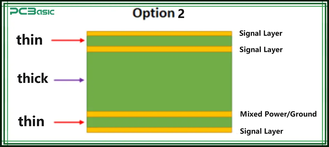


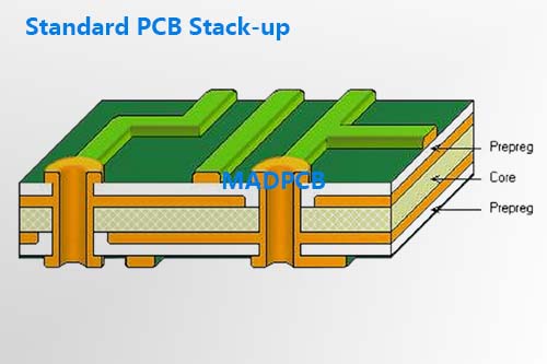


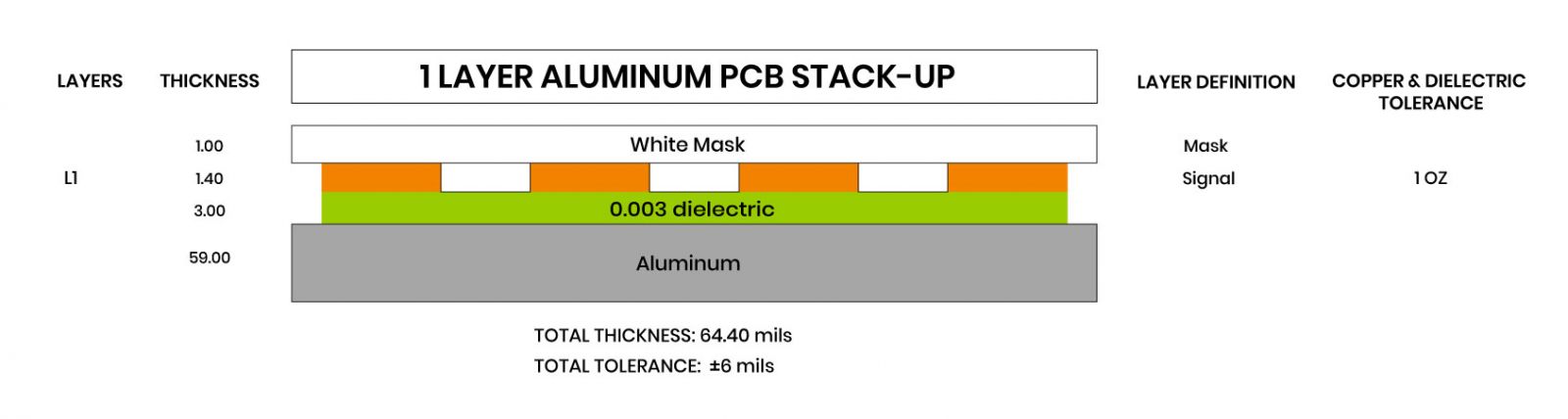
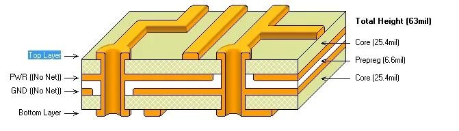


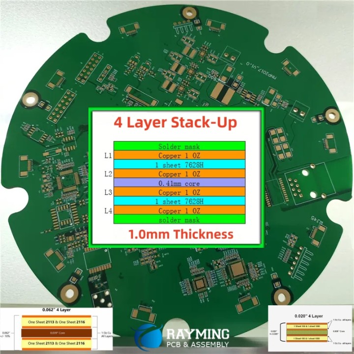


Experience the timeless beauty of 4 layer pcb stackup: thickness, cost & manufacturing process with our curated gallery of vast arrays of images. showcasing the classic style of photography, images, and pictures. designed to evoke timeless elegance. The 4 layer pcb stackup: thickness, cost & manufacturing process collection maintains consistent quality standards across all images. Suitable for various applications including web design, social media, personal projects, and digital content creation All 4 layer pcb stackup: thickness, cost & manufacturing process images are available in high resolution with professional-grade quality, optimized for both digital and print applications, and include comprehensive metadata for easy organization and usage. Our 4 layer pcb stackup: thickness, cost & manufacturing process gallery offers diverse visual resources to bring your ideas to life. Time-saving browsing features help users locate ideal 4 layer pcb stackup: thickness, cost & manufacturing process images quickly. Advanced search capabilities make finding the perfect 4 layer pcb stackup: thickness, cost & manufacturing process image effortless and efficient. Regular updates keep the 4 layer pcb stackup: thickness, cost & manufacturing process collection current with contemporary trends and styles. The 4 layer pcb stackup: thickness, cost & manufacturing process archive serves professionals, educators, and creatives across diverse industries. Multiple resolution options ensure optimal performance across different platforms and applications. Professional licensing options accommodate both commercial and educational usage requirements.