Please enter url.
Login
Logout
Please enter url.
[DIAGRAM] Circuit Diagram Using Nand Gate - MYDIAGRAM.ONLINE
mydiagram.online
source
Comments
Schematic and layout of 1X 2-input NAND gates with (a) GLB applied to ...
Leakage compensation scheme for ultra‐high‐resistance pseudo‐resistors ...
What Computers are Made From
Smart Cities | Free Full-Text | Design, Analysis and Implementation of ...
Schematics of three MEMTJ devices. (a) standard MEMTJ, (b) compact ...
(a) Equivalent RC circuit that models the time-dependent electrical ...
Figure 1 from SRAM Alpha-SER Estimation From Word-Line Voltage Margin ...
Smart Cities | Free Full-Text | Design, Analysis and Implementation of ...
Figure 1 from Common-Centroid Layouts for Analog Circuits: Advantages ...
What does rail-to-rail mean (Rail-to-Rail Op amp) ? | Toshiba ...
(a) Schematic diagram of the DSTATCOM converter and filter structure ...
Mechanism of floating body effect mitigation via cutting off source ...
Figure 10 from Challenges and Solutions of the TFET Circuit Design ...
The Improved Unified Power Quality Conditioner with the Modular ...
Schematic diagram of the proposed SAPG circuit (a) and level down ...
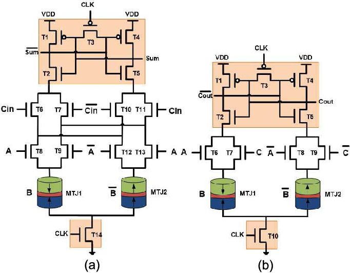
Figure 4 from Area and Energy Efficient Magnetic Full Adder based on ...
Figure 1 from A Multiband, Low Power and Low Phase Noise CMOS Voltage ...
Equivalent circuit of the proposed attenuation‐tunable balanced ...
(a) Schematic diagram of our proposed two-mode coupled circuit QED ...
Sensors | Free Full-Text | A Hybrid Bipolar Active Charge Balancing ...
[PDF] Study and Verification on the Latch-Up Path Between I/O pMOS and ...
(a) Equivalent circuit model of the 2 ? 1 antenna array with the SSIS ...
Decoder structure of joint CAC-ECC scheme. | Download Scientific Diagram
Figure 1 from DC short circuit ride-through strategy for a full-bridge ...
Figure 1 from Energy-Efficient Design of Hybrid MTJ/CMOS and MTJ ...
Part IA Engineering: Digital Circuits and Information Processing
Schematics of a 2 × 2 array of 1T-SRAM cells and a p-channel FBFET ...
True random generator with 2-input XOR-based post-processing unit ...
A 3-Vppd 730-mW Linear Driver IC Using InP HBTs for Advanced Optical ...
Schematic of 6 T CNTFET SRAM Cell. | Download Scientific Diagram
Topology for four CMOS gates. (a) INV. (b) NAND-2. (c) NOR-2. (d) MIN-3 ...
Proposed LRFF design. (a) Complementary pass logic circuit technique ...
Memtransistor (MemTX) crossbar simulation parameters. | Download ...
Circuit and layout for a FinFET IC with horizontal M1 in blue, vertical ...
3Schematics of a a PMOS-input folded cascade opamp for the integrators ...
Nand-Gate-Pinout
8-Input-Nand-Gate
Nand-Gate-Inverter
Nand-Gate-Pin-Diagram
74HC00
CMOS-NOR-Gate
Nand-Layout
Nor-Gate-IC
Universal-Nand-Gate
Nand-Gate-Circuit
IC-Gates
Three-Input-Nand-Gate
NMOS-Nand-Gate
IC-74LS00
Nand-Gate-Transistor
Nand-Gate-Logic-Table


![[PDF] Study and Verification on the Latch-Up Path Between I/O pMOS and ...](https://d3i71xaburhd42.cloudfront.net/25a1c700fc1d6cb210015f31c1dcb1d4a333eaef/1-Figure1-1.png)