


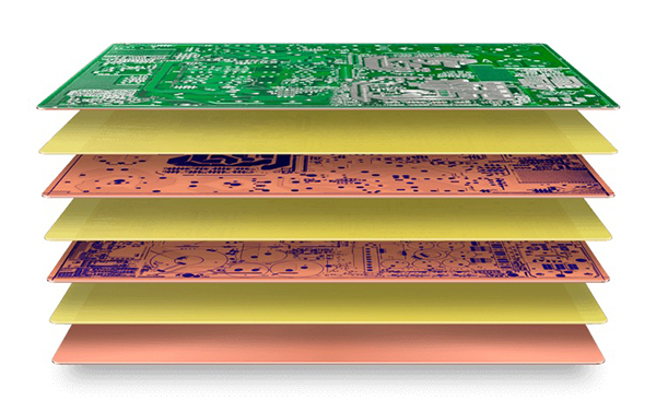
![Multilayer Pcb Design [ from 2 layers to 32 lasers] - Design Your PCB Now](https://www.venture-mfg.com/wp-content/uploads/2019/06/Figure-5-Single-layer-vs-multi-layer-PCB.jpg)


![Your Guide to All PCB Types [Printed Circuit Boards Explained]](https://www.cirexx.com/wp-content/uploads/Multi-Layer.jpg)


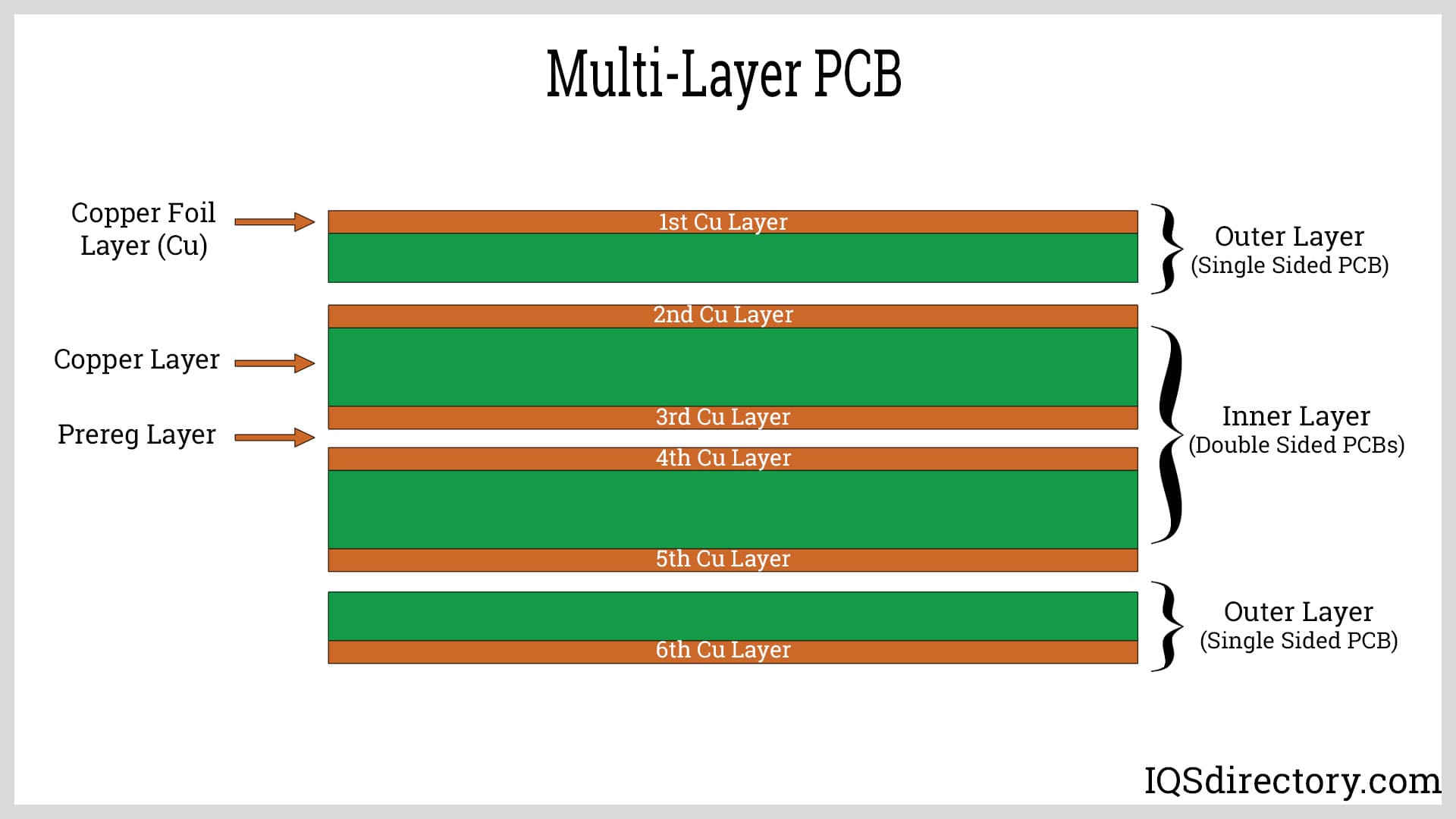
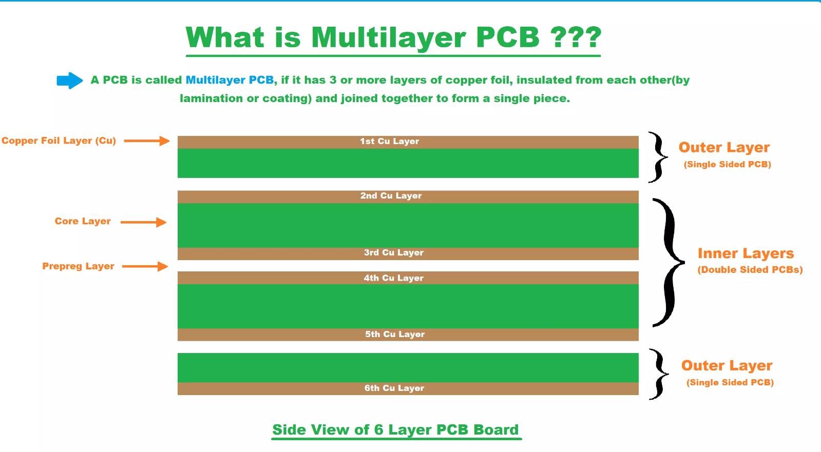
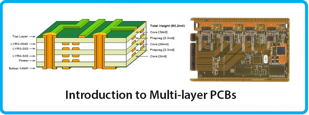
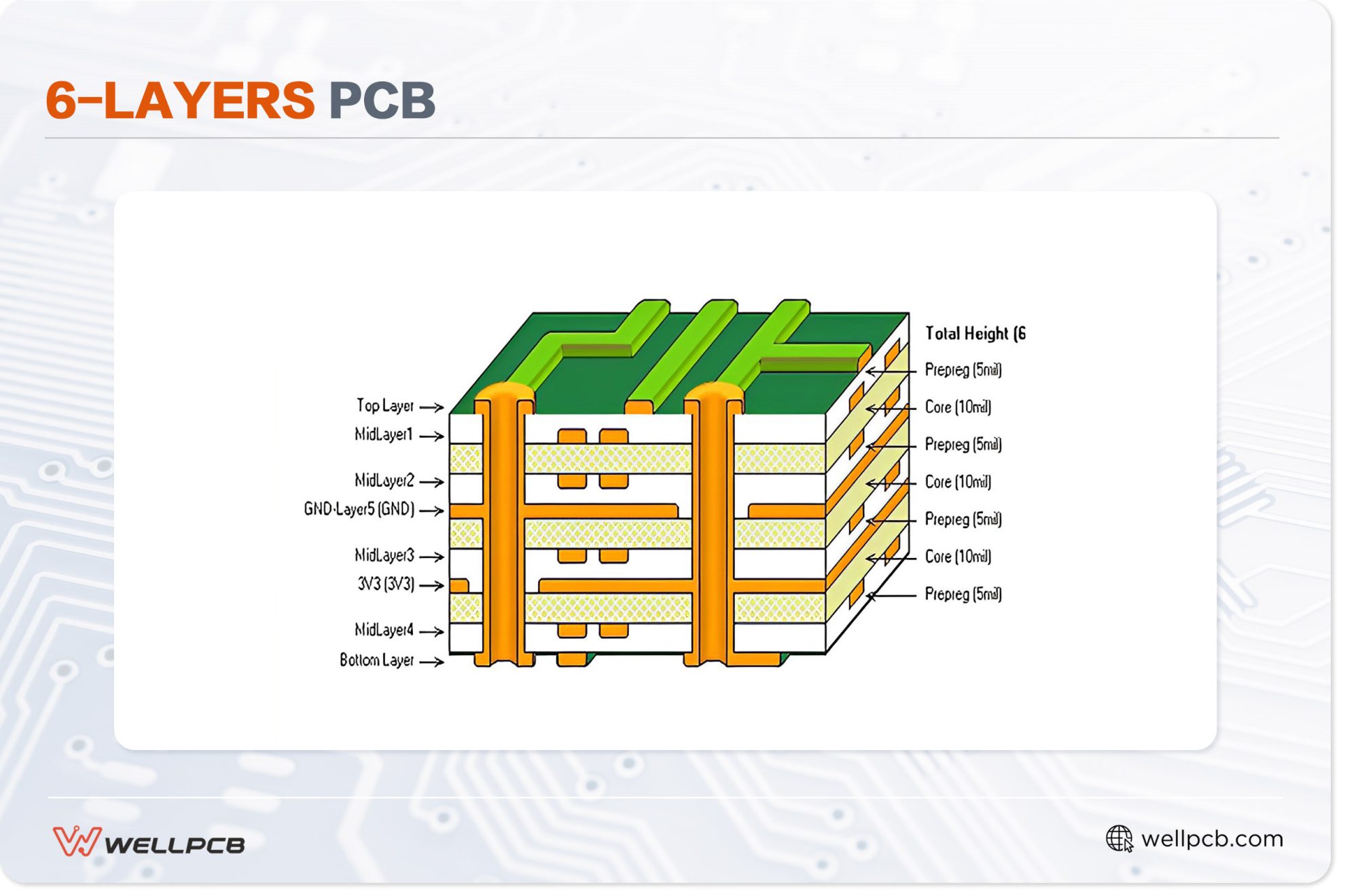
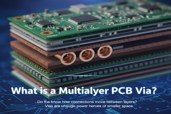
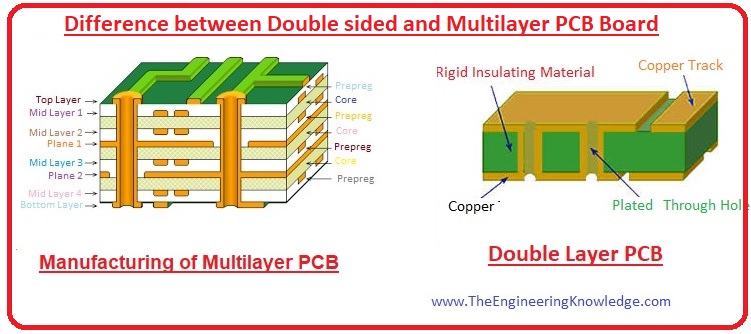
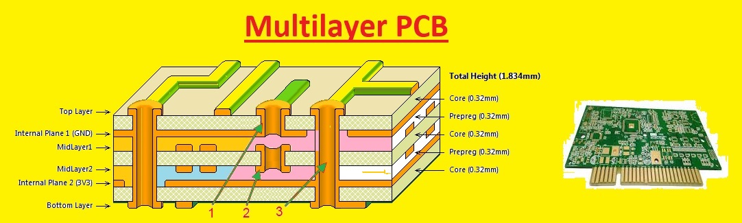
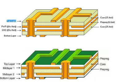
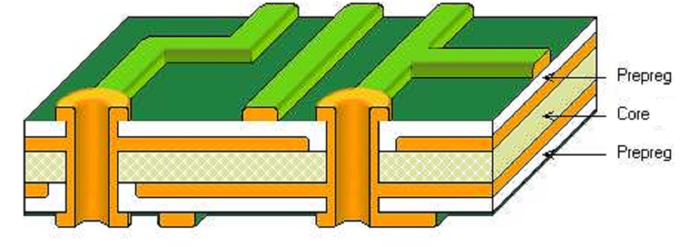
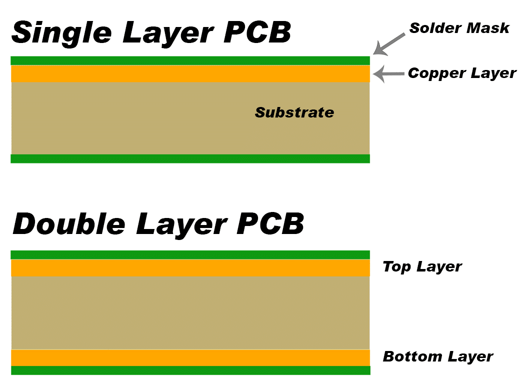
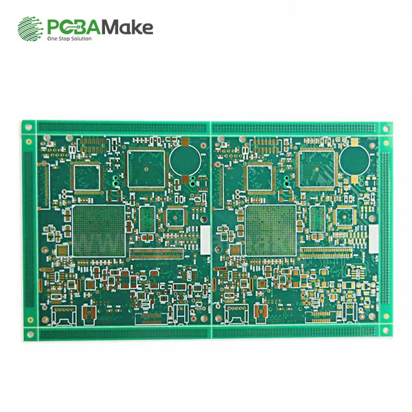
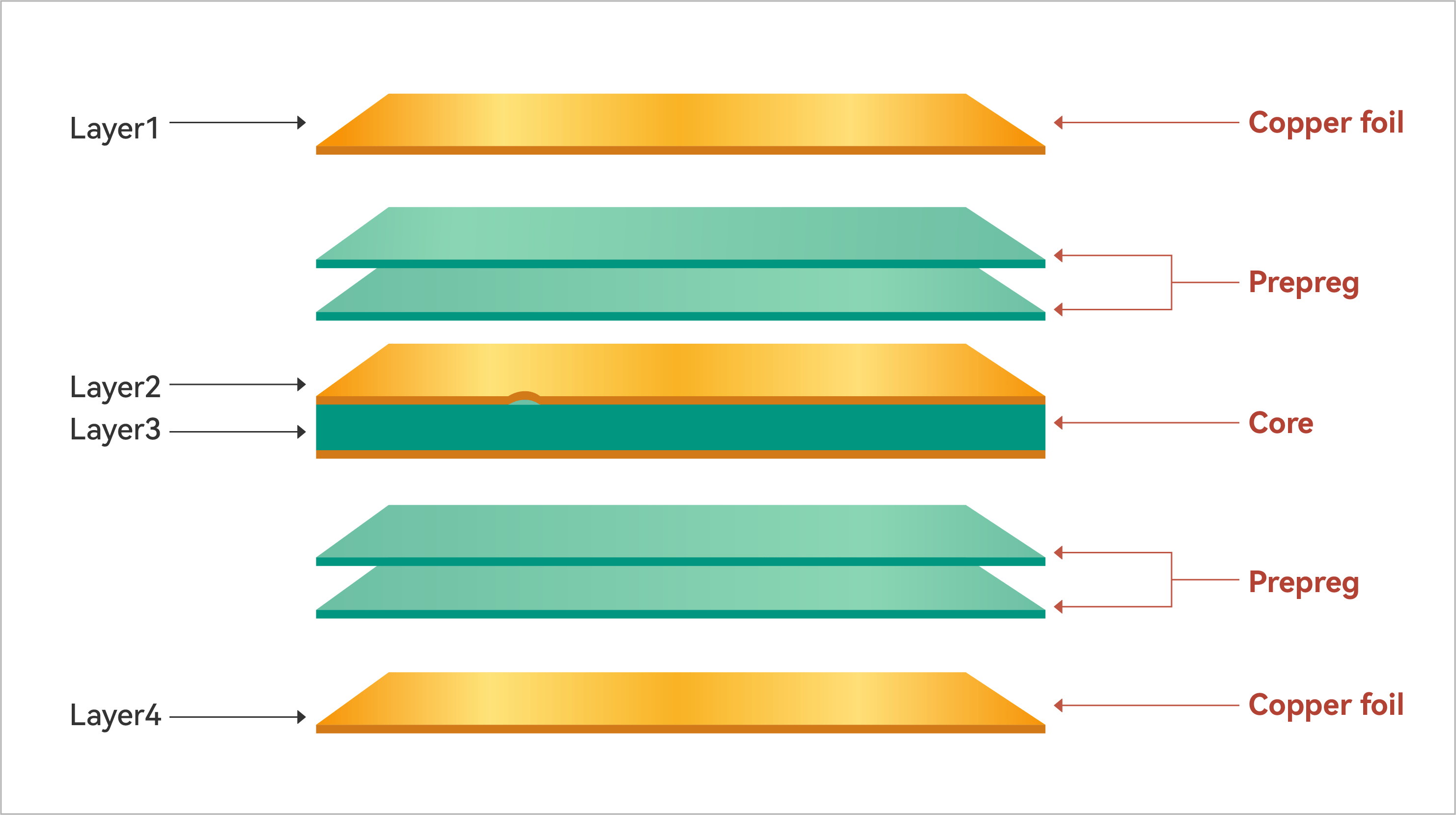
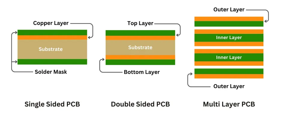
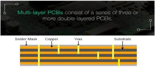
Examine the remarkable technical aspects of why pcbs have multiple layers & what they’re used for? | viasion with substantial collections of detailed images. illustrating the mechanical aspects of photography, images, and pictures. ideal for engineering and scientific applications. Browse our premium why pcbs have multiple layers & what they’re used for? | viasion gallery featuring professionally curated photographs. Suitable for various applications including web design, social media, personal projects, and digital content creation All why pcbs have multiple layers & what they’re used for? | viasion images are available in high resolution with professional-grade quality, optimized for both digital and print applications, and include comprehensive metadata for easy organization and usage. Our why pcbs have multiple layers & what they’re used for? | viasion gallery offers diverse visual resources to bring your ideas to life. Advanced search capabilities make finding the perfect why pcbs have multiple layers & what they’re used for? | viasion image effortless and efficient. Diverse style options within the why pcbs have multiple layers & what they’re used for? | viasion collection suit various aesthetic preferences. Regular updates keep the why pcbs have multiple layers & what they’re used for? | viasion collection current with contemporary trends and styles. Each image in our why pcbs have multiple layers & what they’re used for? | viasion gallery undergoes rigorous quality assessment before inclusion.