Please enter url.
Login
Logout
Please enter url.
What Is Cmos Pmos Nmos For Beginners Part 1 Youtube - vrogue.co
vrogue.co
source
Comments
What is the difference between NMOS, PMOS and CMOS transistors? - Quora
Cross sections of SOI lateral p-i-n diodes lying on (a) microhotplate ...
New PMOS Devices Take a Note on the Low On-Resistance of NMOS - News
Time evolution of QWQDs absorbance spectrum for a) core CdS, b ...
Perovskite Solar Cells: An In-Depth Guide + Comparisons With Other Techs
Fabrication procedure of suspended germanium waveguides with ...
Responsivity and Quantum efficiency of 4H-SiC UV-PDs. | Download ...
Single crystal silicon solar cells of different structure. | Download ...
(Color online) Schematic illustration of the typical device structure ...
͑ Color online ͒ Structure of ͑ a ͒ a device with HRG electrodes and ͑ ...
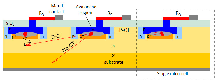
Electronics | Free Full-Text | Bit Error Performance of APD and SPAD ...
Sensors | Free Full-Text | Ion-Sensitive Field-Effect Transistor for ...
Solved Draw charge density, capacitance , and energy band | Chegg.com
Ge photodiode with RMG materials (not to scale) | Download Scientific ...
What is an SiPM and how does it work? | Hamamatsu Photonics
(a) Three-dimensional schematic diagram and (b) cross-section of the ...
Cross section view of the 3-D microring lasers used in the simulation ...
Graphene−silicon−graphene Schottky junction photodetector with field ...
[PDF] Bimodal Waveguide Interferometer RI Sensor Fabricated on Low-Cost ...
Classification of electrical control approaches. (a) Application of ...
(Color online) Schematic diagram of two-step lithography process ...
Dynamic On-Resistance in GaN Power Devices: Mechanisms ...
The Yamazaki-Teiichi Prize | The 13th (2013) Yamazaki-Teiichi Prize ...
Schematic cross-sectional views of the key fabrication process steps of ...
Nanomaterials | Free Full-Text | A Design of High-Efficiency: Vertical ...
Phenomenon of latchup in the integrated circuits. | Download Scientific ...
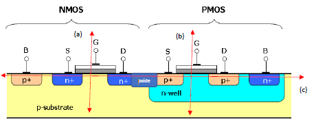
Schematics of a (a) MOSFET with p-type silicon as a base substrate ...
10 Schematic of nanometer-scale QD-OLED structure that contains ...
Downscaling Classical MOSFET | SpringerLink
Schematic representation of: a) BCE or LO, b) ESL processes; c) and d ...
Schematic diagrams of the (a) conventional Ga 2 O 3 MOSFET and (b) Ga 2 ...
Graphene Field-Effect Transistors | by Charlotte Brown | Nerd For Tech ...
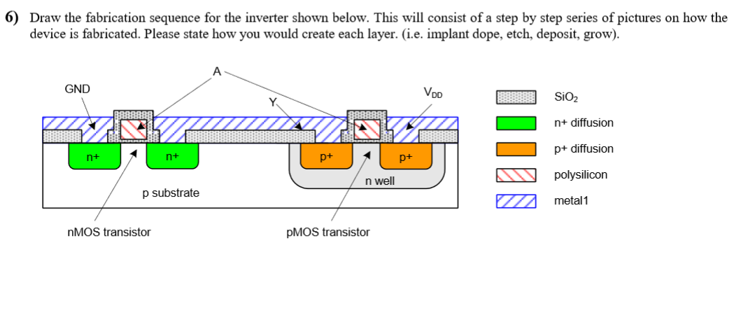
Solved 6) Draw the fabrication sequence for the inverter | Chegg.com
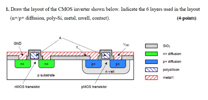
SOLVED: Draw the layout of the CMOS inverter shown below. Indicate the ...
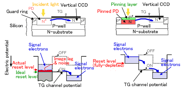
(Color online) Schematic cross-sectional diagram of the PPD and the TG ...


![[PDF] Bimodal Waveguide Interferometer RI Sensor Fabricated on Low-Cost ...](https://d3i71xaburhd42.cloudfront.net/f0c7533d96e0ddf288d39cb9ba1bd7b4241a7b1c/6-Figure3-1.png)