Please enter url.
Login
Logout
Please enter url.
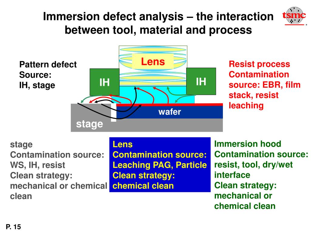
Typical immersion defect types and on wafer distribution:... | Download ...
researchgate.net
source
Comments
(PDF) The rapid introduction of immersion lithography for NAND Flash ...
Steps involved in the fabrication of silicon micro-patterns using ...
PPT - Applications of Chemical Engineering Principles to Thin Film ...
Step-by-step classification of the defects. | Download Scientific Diagram
Reinforcement of a dodecylacrylate plasma polymer by admixture of a ...
(a) Planar cross-section and (b) longitudinal cross-section of the ...
hoP defect Escape hypothesis illustrated | Download Scientific Diagram
(PDF) Diamond-Like Carbon (DLC) Coatings: Classification, Properties ...
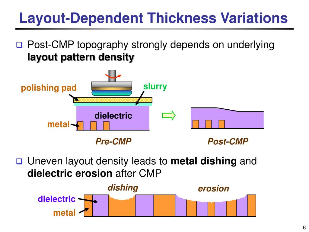
PPT - Novel Wire Density Driven Full-Chip Routing for CMP Variation ...
A top-level timeline showing a phased approach to the Cosmic Explorer ...
Photocatalytic Membranes Toward Practical Environmental Remediation ...
LED, BGA, and QFN Inspection - X-Ray Inspection for SMT Quality Assur…
tablet defects
Dry etch-based BCB cap process | Download Scientific Diagram
Polymers | Free Full-Text | Review on Blueprint of Designing Anti ...
STANFORD Advanced LIGO High-Power Photodiodes David Jackrel, PhD ...
Online sealing procedure of SF6 leakage of GIS | Download Scientific ...
Process flow for the fabrication of conductometric gas sensor substrate ...
Schematic of IPMNs fabrication process. | Download Scientific Diagram
Near Void-Free Assembly Development of Flip Chip Using No-Flow ...
Magnetic field simulation applied in the process of deposition of the ...
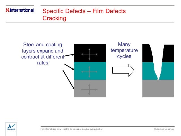
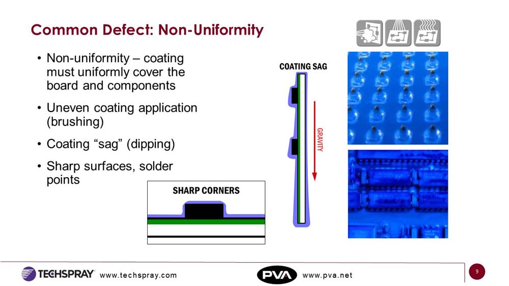
coating defects
PPT - Process stability control for immersion lithography PowerPoint ...
A Braille display-based microfluidic cell culture and assay system. The ...
WEBINAR: Conformal Coating Defects -- How To Diagnose, Repair & Prevent ...
Key steps of specimen preparation for prestressed (top) and unstressed ...
Frontiers | Abnormal Resting-State Functional Connectivity in the Whole ...
Schematic illustration of the templating procedures for making moth-eye ...
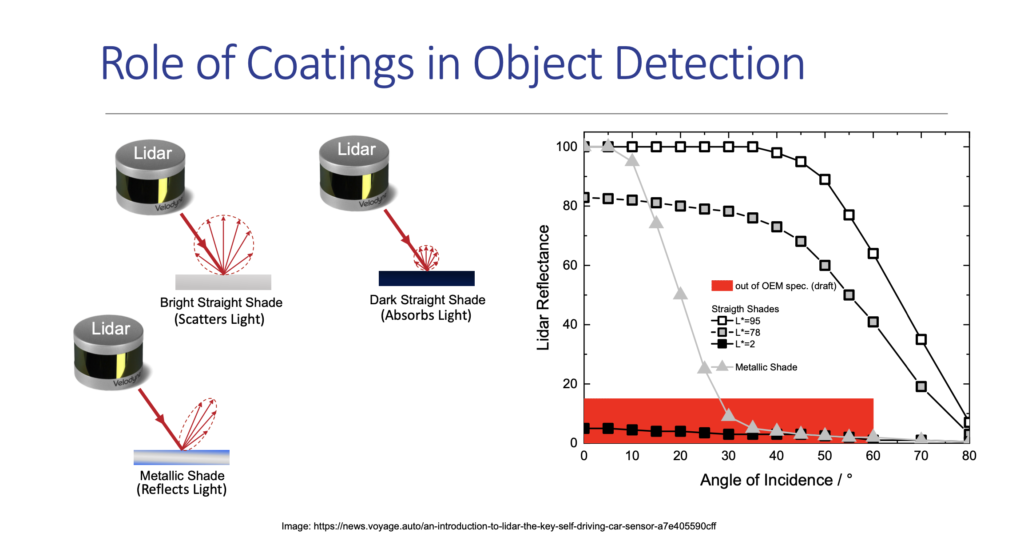
Panelists explore lidar’s promises, challenges during CIC presentation ...
The four pillars of quality improvement using the example of automated ...
Technology development fields of the additive manufacturing process ...
Schematic of improved wafer bonding/debonding technique for BCB ...
Laser cladding systems: (a) components of the experimental setup; (b ...
nanoHUB.org - Resources: ME 517 Lecture 04: Microfabrication ...
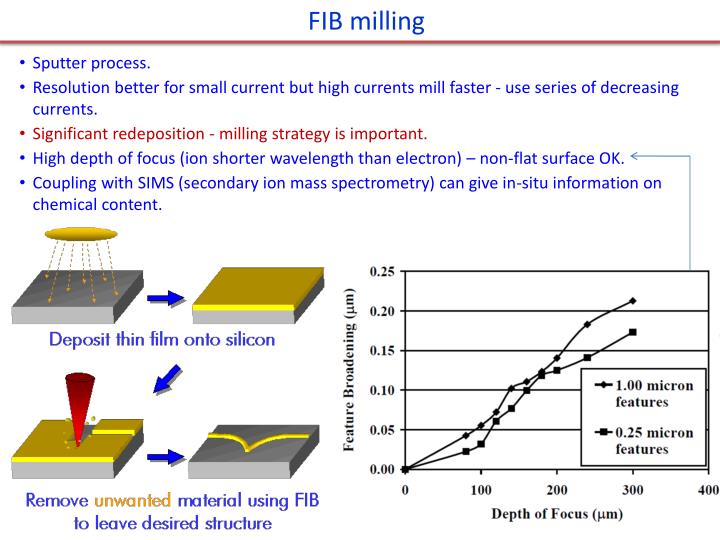
PPT - Focused ion beam (FIB) PowerPoint Presentation - ID:2018793
Semiconductor-Wafer-Defects
SIC-Wafer
Silicon-Wafer-Icon
Wafer-Inspection-System
Wafer-Chip
Wafer-Arcing-Defect
Wafer-Process-Flow
Dummy-Wafer
Silicon-Wafer-Surface-Defect
Epi-Defect-Wafer
Wafer-Acring-Defect
Wafer-Die
Wafer-SEM-Image
Silicon-Carbide-Wafer
Wafer-Inspection-Equipment
SIC-Wafer-Orientation