

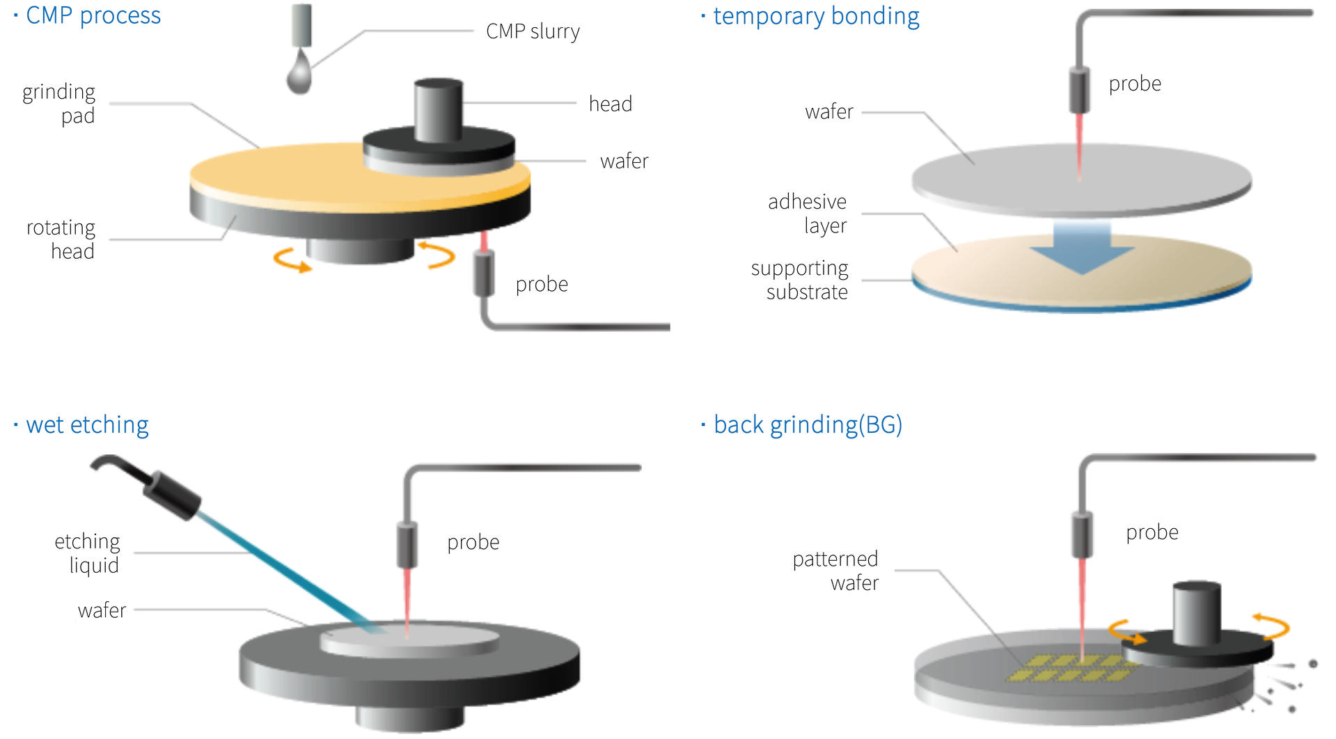


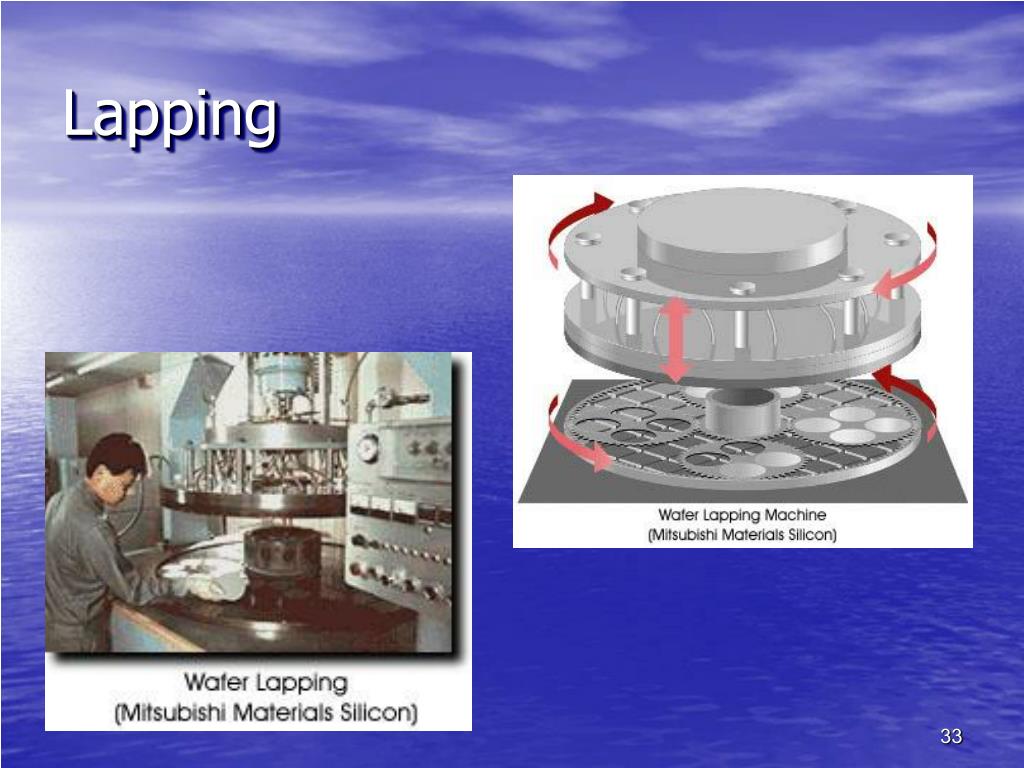


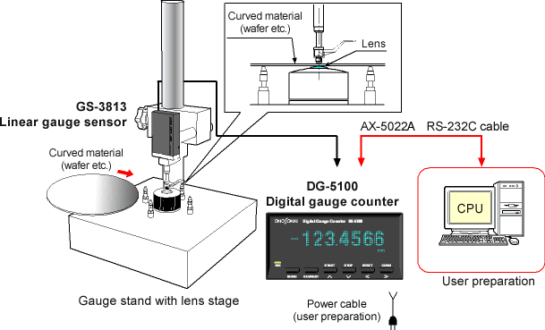


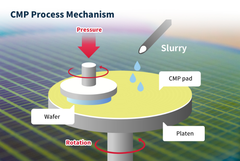
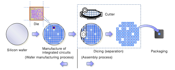
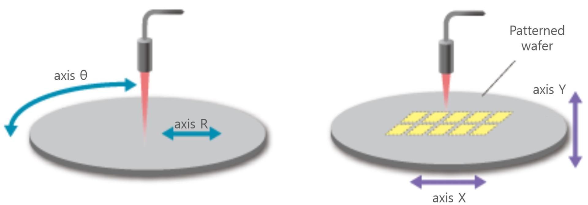
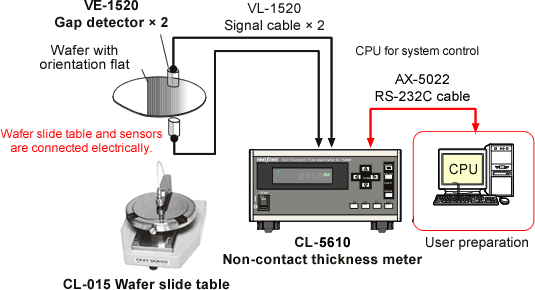
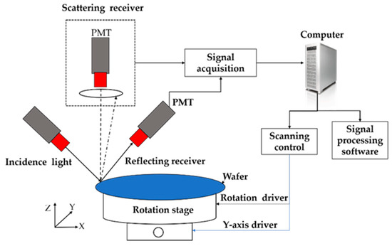
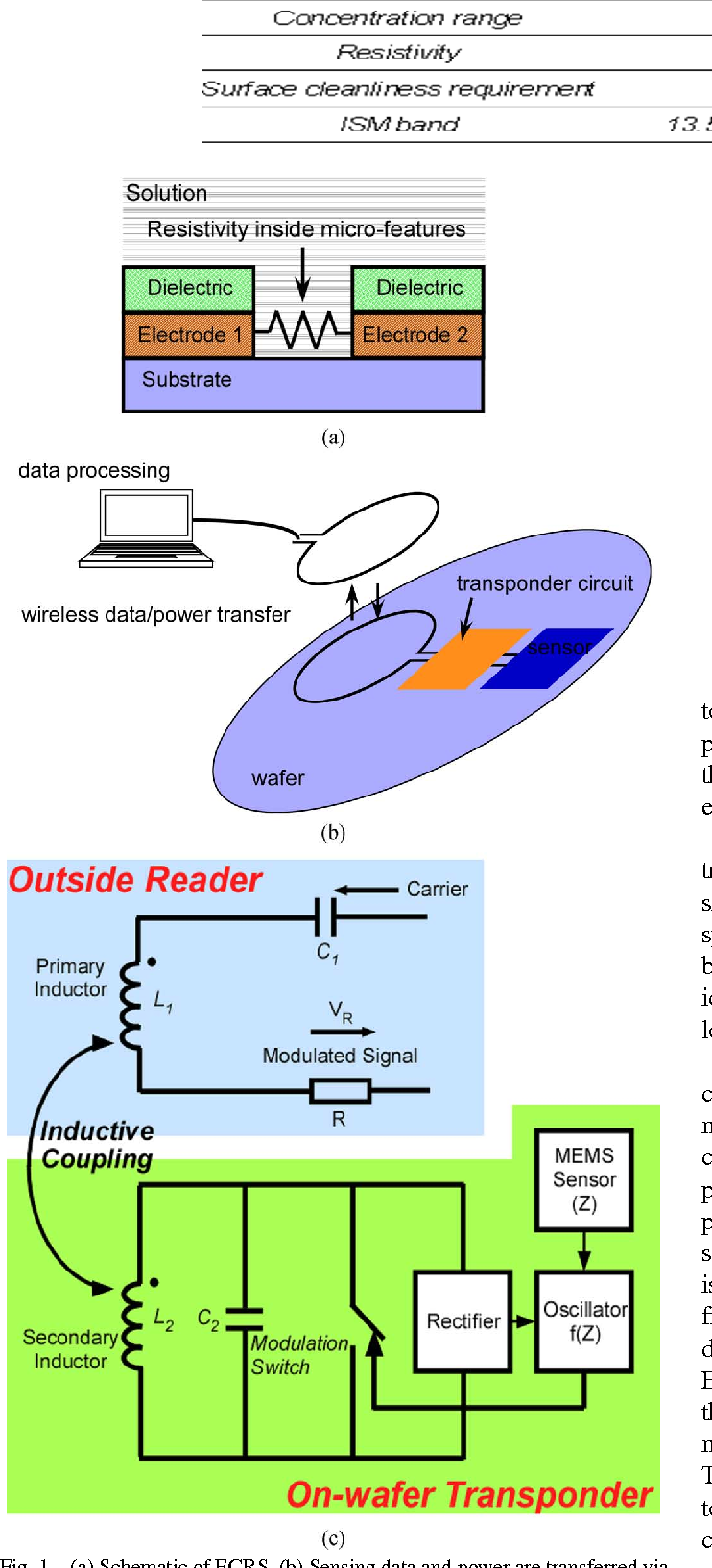
.png)


.jpg)


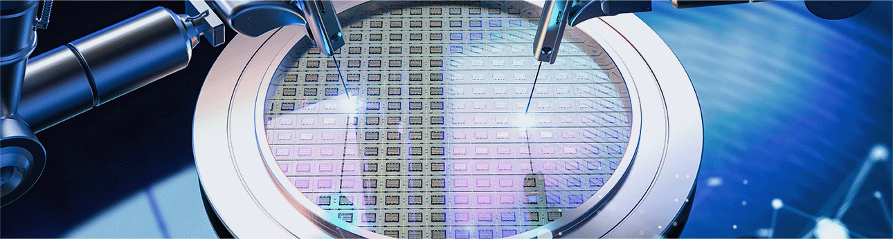

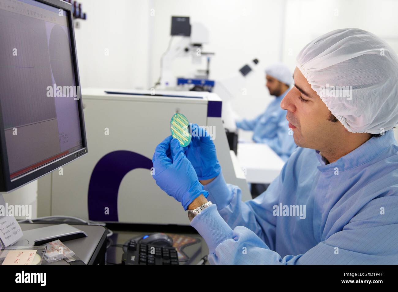
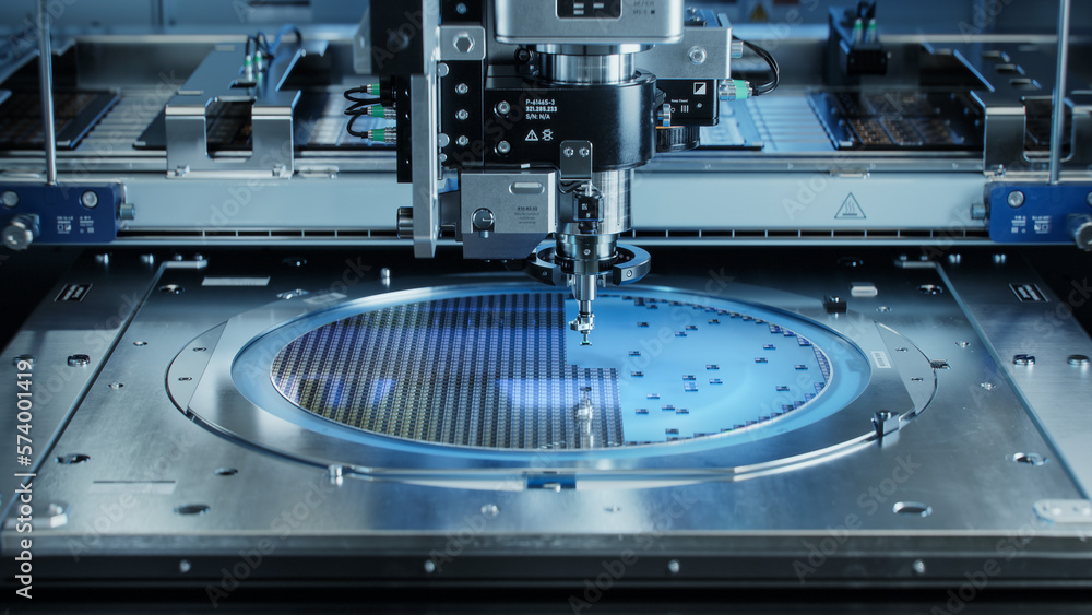

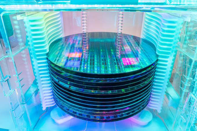


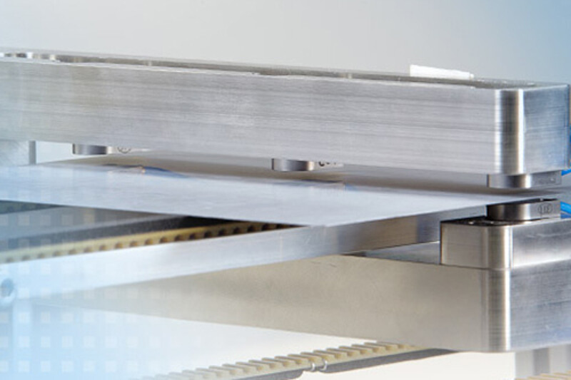
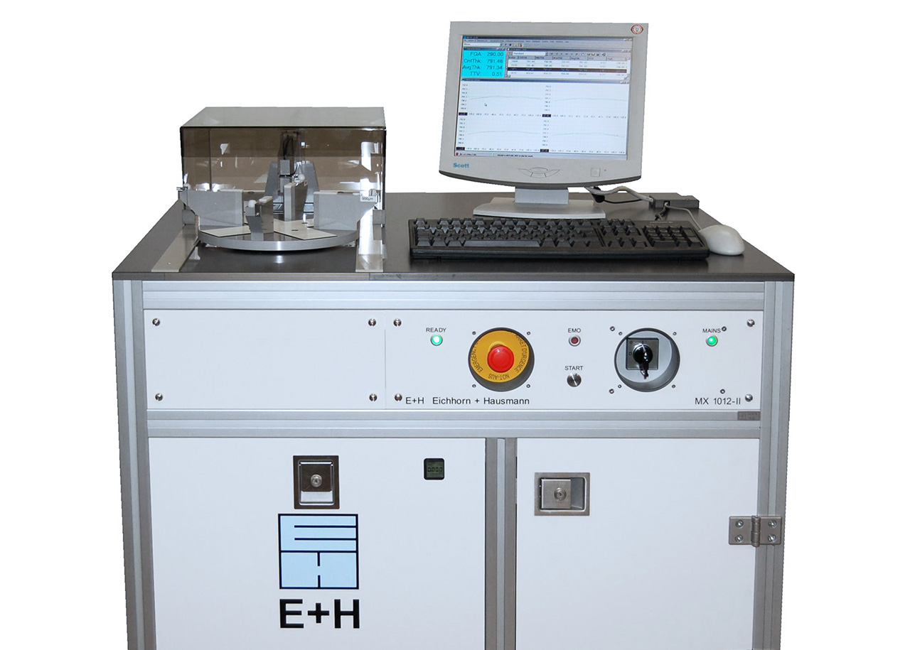
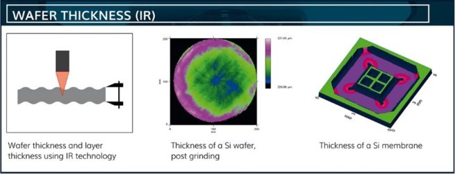
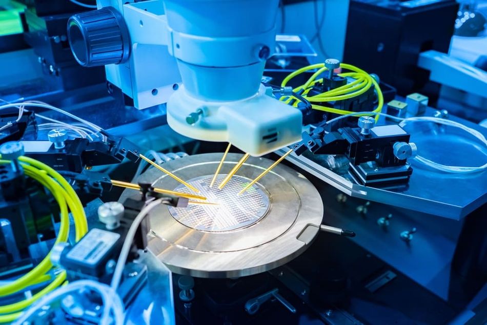
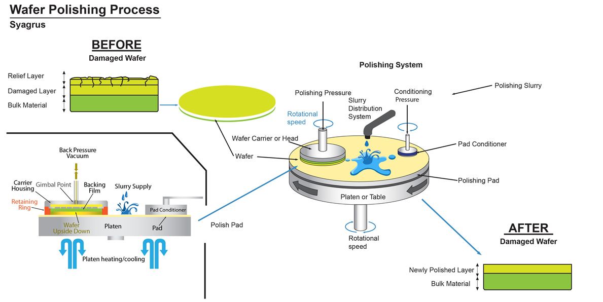
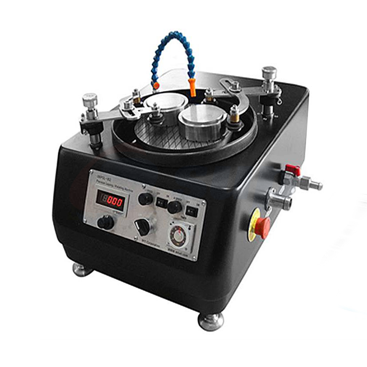
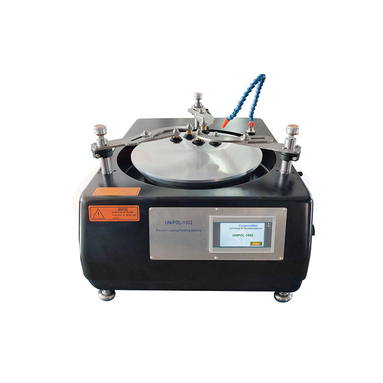
Document reality with our remarkable real-time thickness monitoring in semiconductor wafer lapping collection of extensive collections of authentic images. authentically documenting photography, images, and pictures. designed to preserve authentic moments and stories. Browse our premium real-time thickness monitoring in semiconductor wafer lapping gallery featuring professionally curated photographs. Suitable for various applications including web design, social media, personal projects, and digital content creation All real-time thickness monitoring in semiconductor wafer lapping images are available in high resolution with professional-grade quality, optimized for both digital and print applications, and include comprehensive metadata for easy organization and usage. Our real-time thickness monitoring in semiconductor wafer lapping gallery offers diverse visual resources to bring your ideas to life. Comprehensive tagging systems facilitate quick discovery of relevant real-time thickness monitoring in semiconductor wafer lapping content. The real-time thickness monitoring in semiconductor wafer lapping archive serves professionals, educators, and creatives across diverse industries. Instant download capabilities enable immediate access to chosen real-time thickness monitoring in semiconductor wafer lapping images. Whether for commercial projects or personal use, our real-time thickness monitoring in semiconductor wafer lapping collection delivers consistent excellence. Cost-effective licensing makes professional real-time thickness monitoring in semiconductor wafer lapping photography accessible to all budgets. Advanced search capabilities make finding the perfect real-time thickness monitoring in semiconductor wafer lapping image effortless and efficient.