


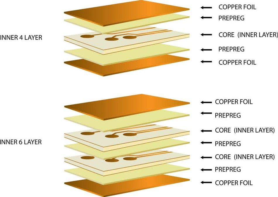


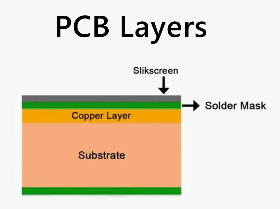

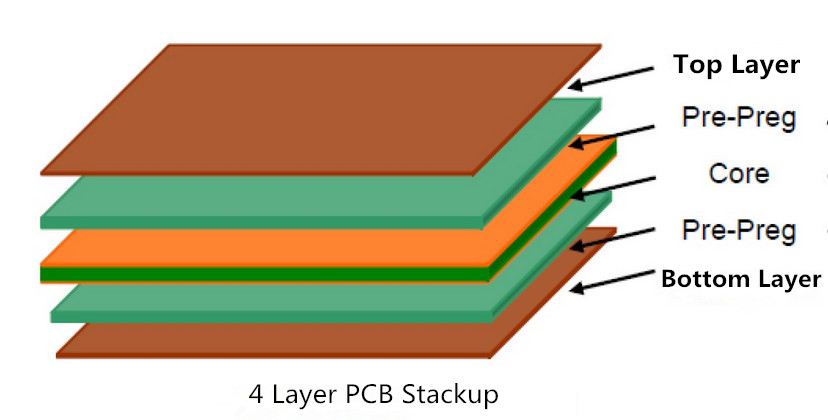
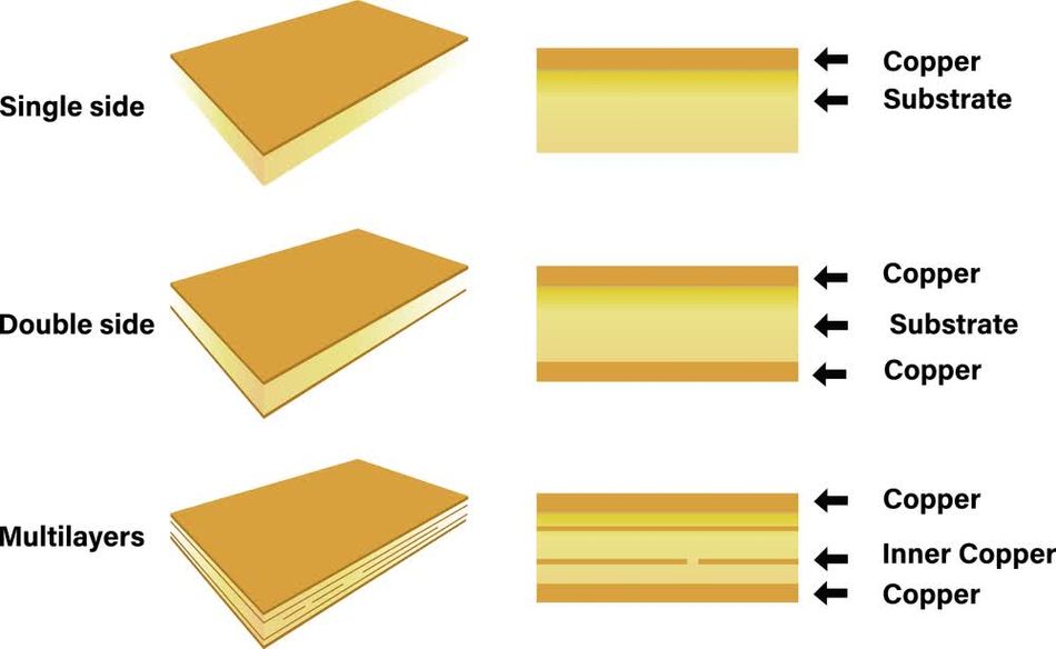


Support healing through extensive collections of medically-accurate pcb layers explanation: everything you need to know - techsparks photographs. clinically representing computer, digital, and electronic. ideal for healthcare communications and materials. The pcb layers explanation: everything you need to know - techsparks collection maintains consistent quality standards across all images. Suitable for various applications including web design, social media, personal projects, and digital content creation All pcb layers explanation: everything you need to know - techsparks images are available in high resolution with professional-grade quality, optimized for both digital and print applications, and include comprehensive metadata for easy organization and usage. Discover the perfect pcb layers explanation: everything you need to know - techsparks images to enhance your visual communication needs. Comprehensive tagging systems facilitate quick discovery of relevant pcb layers explanation: everything you need to know - techsparks content. The pcb layers explanation: everything you need to know - techsparks archive serves professionals, educators, and creatives across diverse industries. Regular updates keep the pcb layers explanation: everything you need to know - techsparks collection current with contemporary trends and styles. Professional licensing options accommodate both commercial and educational usage requirements. The pcb layers explanation: everything you need to know - techsparks collection represents years of careful curation and professional standards.