Please enter url.
Login
Logout
Please enter url.
varză precipitaţii Contractant jk flip flop internal circuit ști ...
glou-glou.fr
source
Comments
J-K Flip-flop And T-Flip-flop || Sequential Logic || Bcis notes
Fibonacci LFSR block | Download Scientific Diagram
Schematic of the 1T1R RRAM cell. The capacitor of the conventional ...
Use the T flip flop design to write structural VHDL | Chegg.com
Digital Electronics Section 11 - Electronics and Communication ...
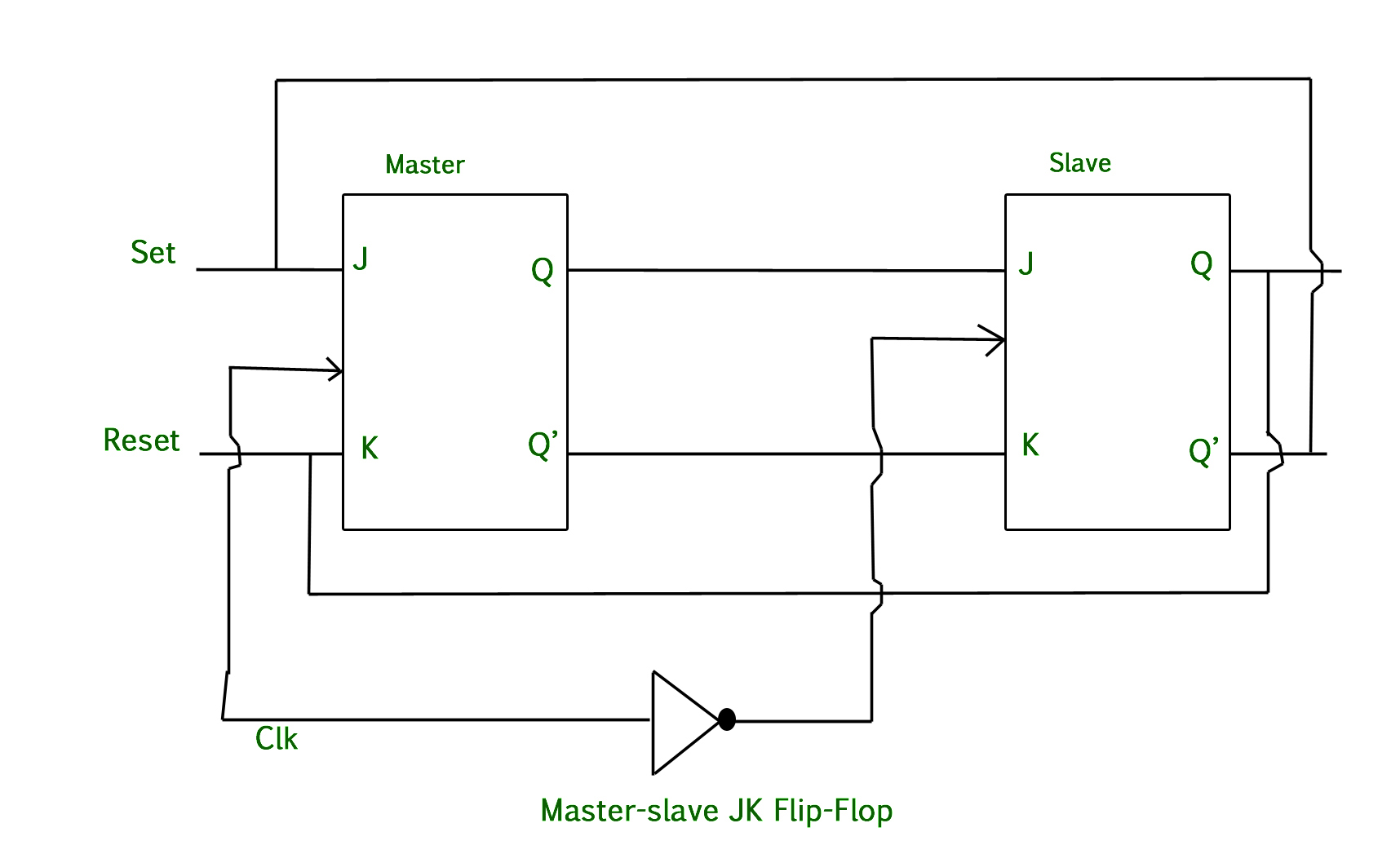
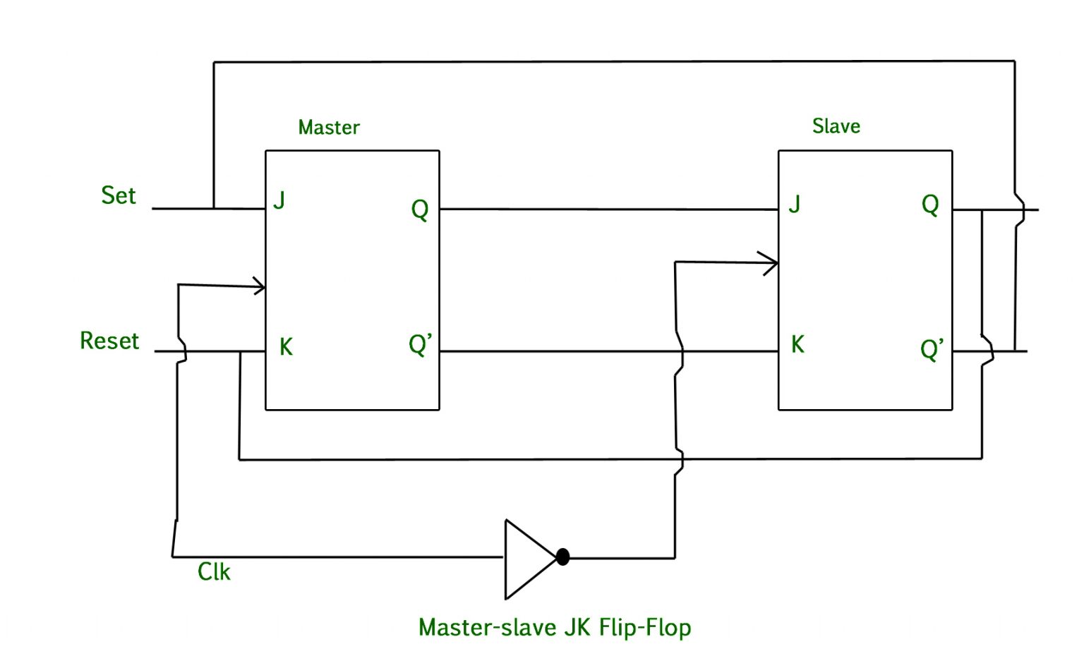
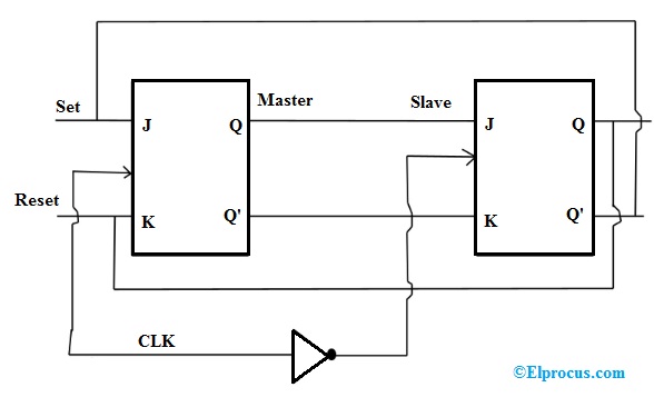
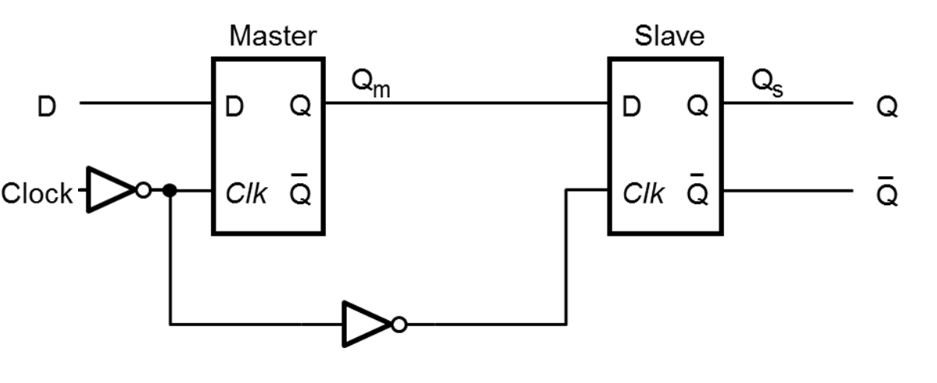
What is a Master-Slave Flip Flop: Circuit Diagram and Its Working
Speed up of circuit using sensitization functions | Download Scientific ...
Schematic diagram of Dual sleep | Download Scientific Diagram
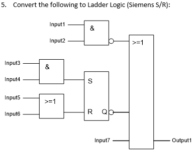
Solved 5. Convert the following to Ladder Logic (Siemens | Chegg.com
Steam Community :: Guide :: Creating complex logic devices with BEE2 ...
Clock Tree Guidances for better Clock Tree Synthesis - Technology@Tdzire
Is the working of a master slave JK FF using nor and nand latch the ...
Are CMOS memes legal? : r/LogicGateMemes
Class Notes for Computer Architecture
Compile Code Conditionally for Variations of Component Represented ...
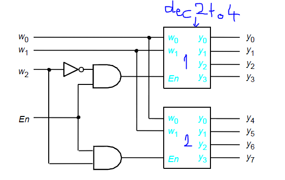
2 To 4 Decoder To 3 To 8 Decoder - slideshare
Figure 2 from A low-voltage, Low-Power 4-bit BCD adder, designed using ...
Digital Circuits - Shift Registers
Comparator - Designing 1-bit, 2-bit and 4-bit comparators using logic gates
Chapter 6 – Flip-Flops, and Registers
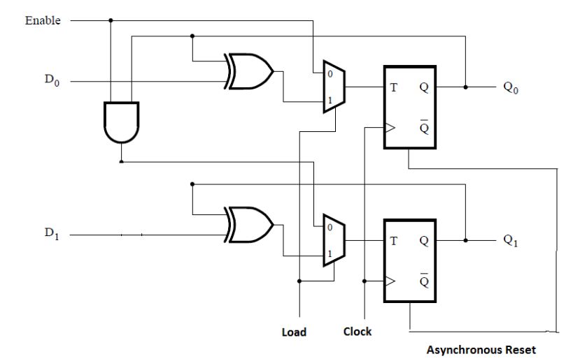
Vhdl Program For 8 Bit Up Down Counters Images
Proposed dual-rail delay-insensitive bi-directional asynchronous ...
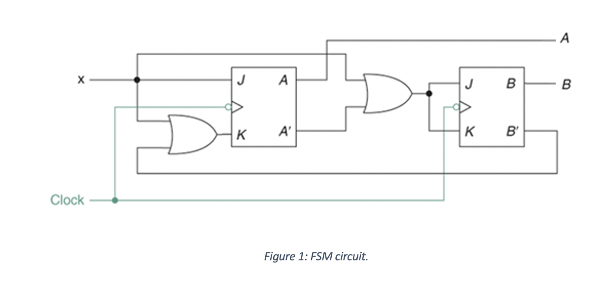
Solved Derive the state table and state diagram of this | Chegg.com
Lecture Notes for Computer Systems Design
Constraining Multi-Cycle Path in Synthesis – VLSI Tutorials
CSE 370 Assignment 7 Solutions
LogicGates | ATMakers
Draw The Circuit Diagram Of Jk Master Slave Flip Flops - Circuit Diagram
Verilog Test Bench Code For D Flip Flop | amberandconnorshakespeare
Block diagram of the CAB algorithm for GPS interference suppression ...
Solved (a) Determine the circuit’s characteristic equations. | Chegg.com
Combinational Logic Input Reverse the design | Chegg.com
Block diagram of 4-bit Ripple Carry Adder | Download Scientific Diagram
post-processing unit. | Download Scientific Diagram
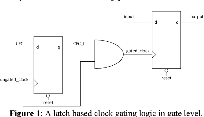
Figure 1 from Clock gating assertion check: An approach towards ...
Jk-Flip-Flop-State-Diagram
Jk-Flip-Flop-Equation
Jk-Flip-Flop-Using-CMOS
Flip-Flop-Timing-Diagram
Jk-Flip-Flop-with-Clear
D-Flip-Flop-Clock
Jk-Flip-Flop-Logic-Diagram
Flip-Flop-Truth-Table
Clocked-Jk-Flip-Flop
Circuit-Diagram-of-Jk-Flip-Flop
Jk-Flip-Flop-Preset-and-Clear
Sr-Flip-Flop-vs-Jk-Flip-Flop
Edge-Triggered-Flip-Flop
Flip-Flop-with-Transistors
Negative-Edge-Triggered-Jk-Flip-Flop
Jk-Flip-Flop-with-Reset