Please enter url.
Login
Logout
Please enter url.
Figure 1 from Development of Nanoimprint Lithography Template Materials ...
semanticscholar.org
source
Comments
Figure 3 from Flip-chip bonding alignment accuracy enhancement using ...
Figure 1 from Small Pitch, High Aspect Ratio Via-Last TSV Module ...
Inkjet printing and lamination bonding process flow. | Download ...
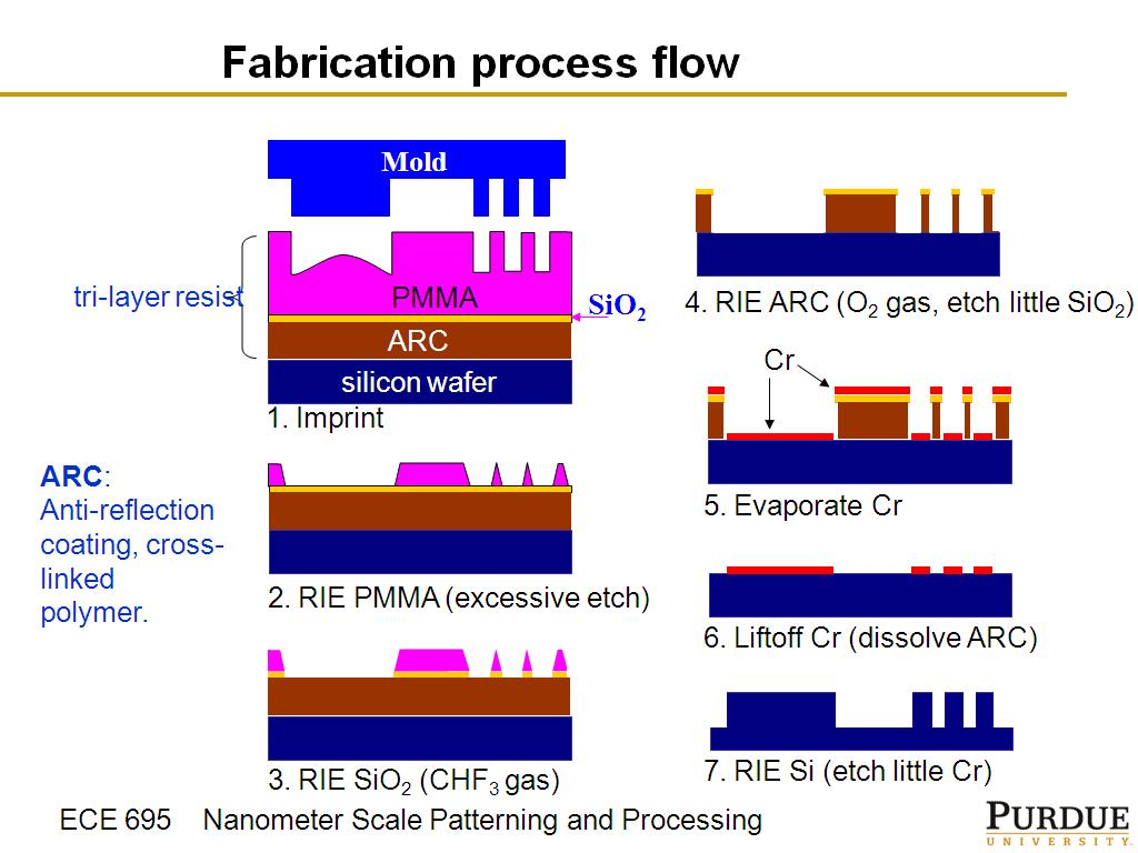
nanoHUB.org - Resources: ECE 695Q Lecture 34: Nanoimprint Lithography ...
Mechanostimulation of Multicellular Organisms Through a High-Throughput ...
Scanning Magnetometry with NV Centers in Diamond | Semantic Scholar
(a) A schematic diagram showing the structure of a Y shaped micro fl ...
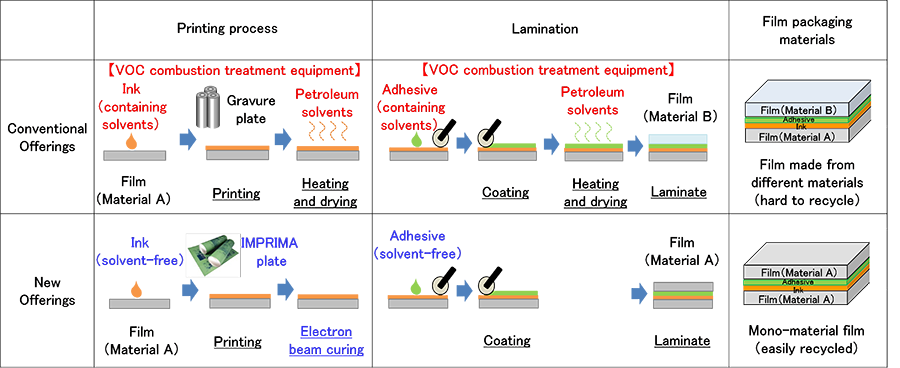
Toray, Mitsui Chemicals and Kumagai Put People and the Planet First by ...
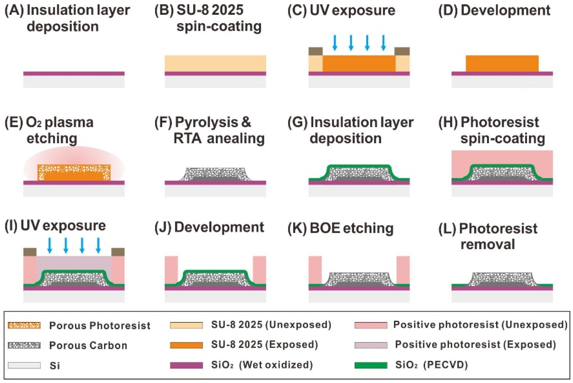
Sensors | Free Full-Text | Hierarchical Porous Carbon Electrodes with ...
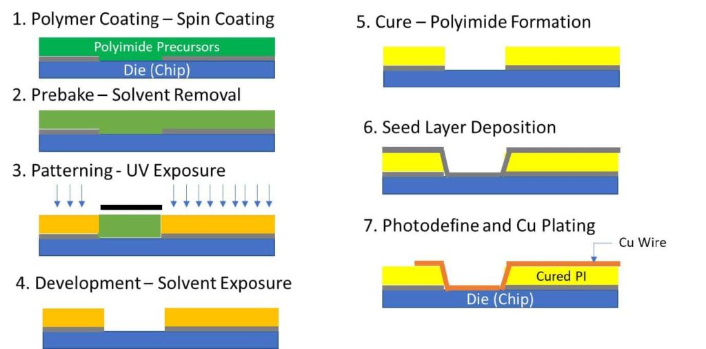
Advanced Semiconductor Polyimides Enabling More than Moore | Halocarbon
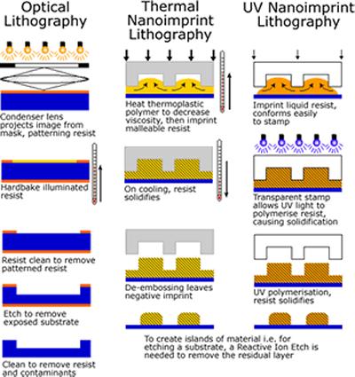
Nanoimprint lithography process development | Engineering | University ...
Photoresponsive wettability switching of TiO2‐coated micropillar arrays ...
A parametric study of ICP-RIE etching on a lithium niobate substrate ...
Application of microneedle patches for drug delivery; doorstep to novel ...
Oriented Halide Perovskite Nanostructures and Thin Films for ...
Nanofluidic device microfabrication. The microfabrication process ...
6.6.1 Lithography
Micromachines | Free Full-Text | The Design and Fabrication of a MEMS ...
All-polymer photonic sensing platform based on whispering-gallery mode ...
Figure 1 from Development of wafer level underfill materials and ...
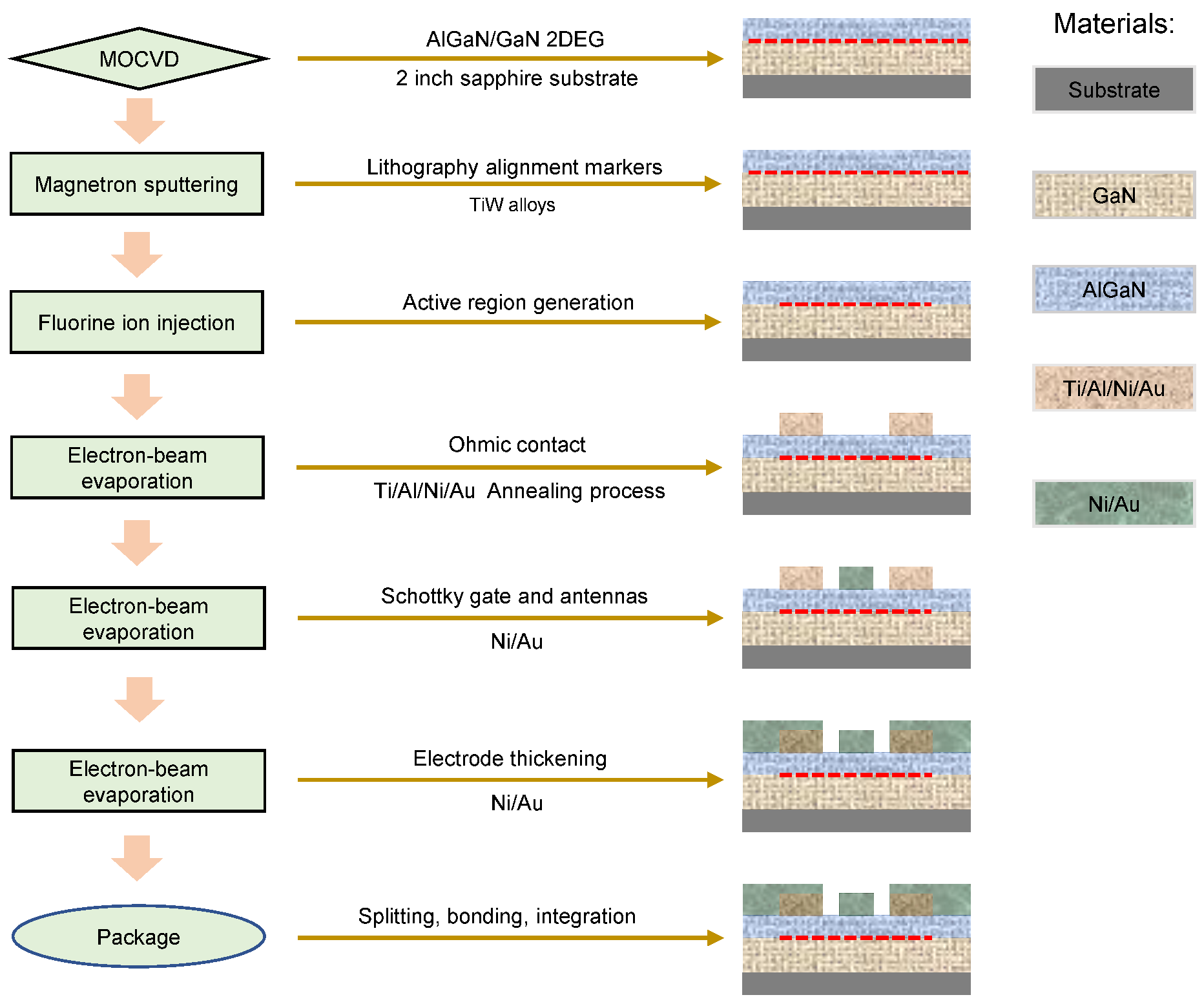
A Novel Approach for Room-Temperature Intersubband Transition in GaN ...
Schematic procedure of the sloped microchannels on Si substrate ...
Fabrication of VOFET devices. In each subfigure, the top is a top view ...
Flowchart for fabricating micro temperature and voltage sensors ...
Schematic drawings of nanocomposite and nanostructured PDMS fabrication ...
Applications of lasers: A promising route toward low-cost fabrication ...
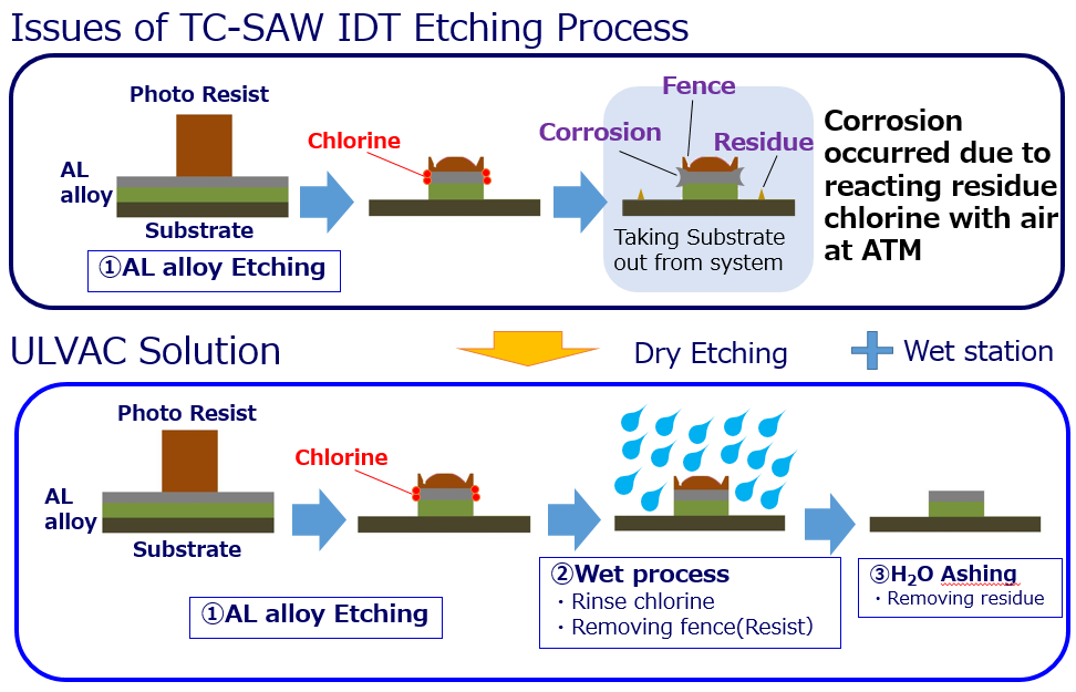
Process technology for SAW device - ULVAC
Fabrication steps of polymer thermo-optic switch. | Download Scientific ...
Schematic of fabrication technology of PDMS platform with barriers and ...
nanoHUB.org - Resources: Nanometer-Scale III-V Electronics: from ...
Schematic for the two-step lithography used to make the VO 2 -covered ...
Electronics | Free Full-Text | Experimental Realization of 16-Pixel ...
2D Material Bubbles: Fabrication, Characterization, and Applications ...
Polymers | Free Full-Text | Dielectrophoretically Assembled SWCNTs ...
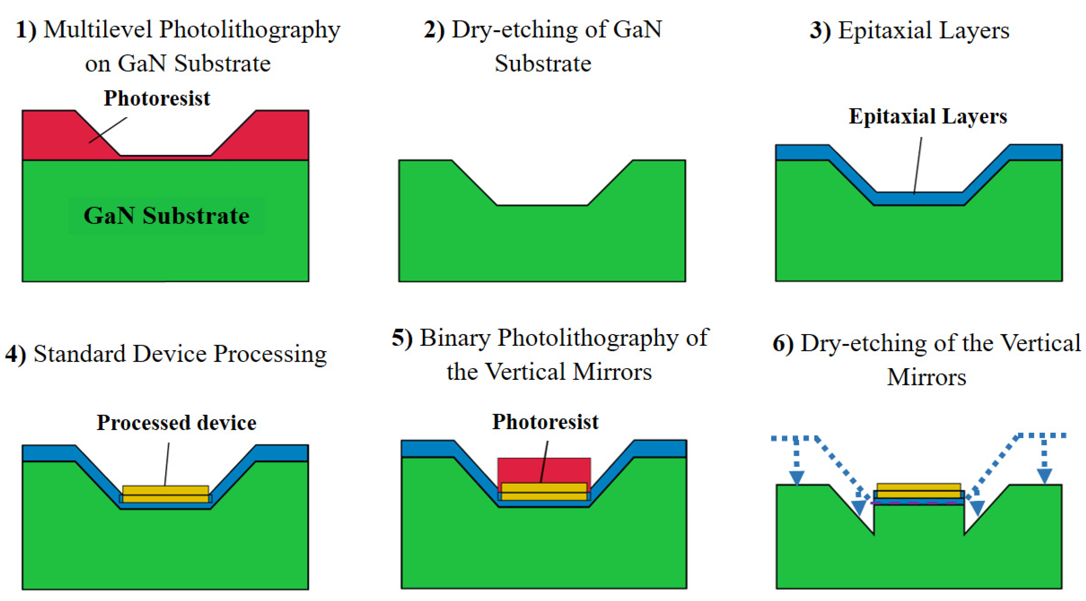
Micromachines | Free Full-Text | Monolithic 45 Degree Deflecting Mirror ...