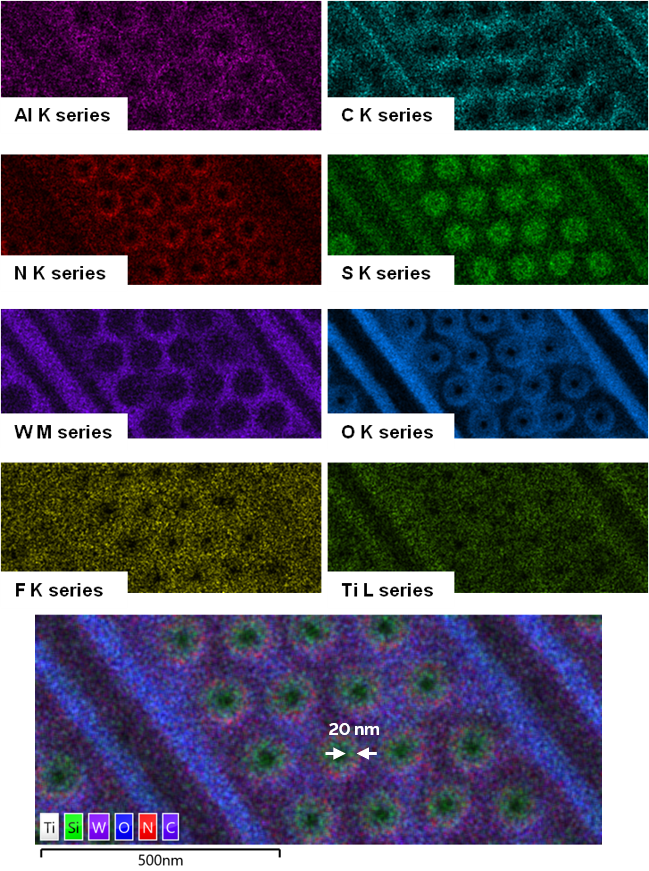
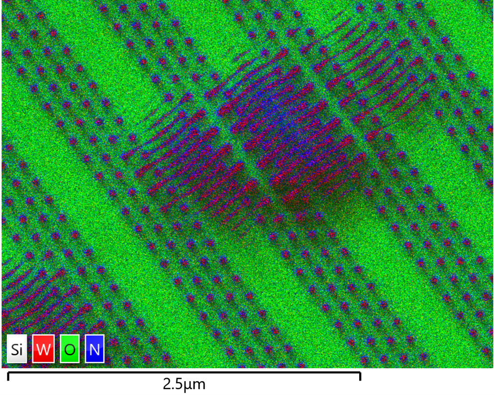
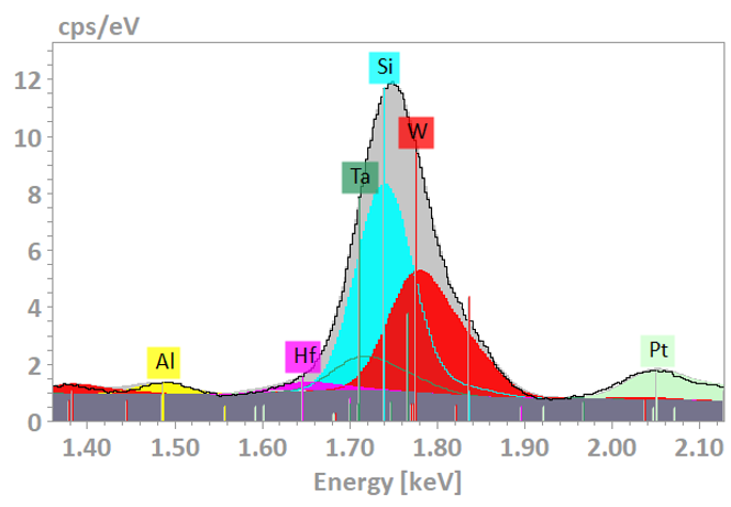
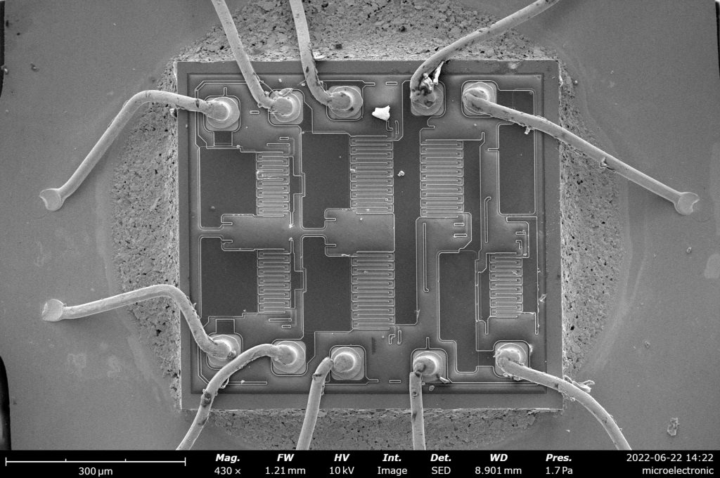
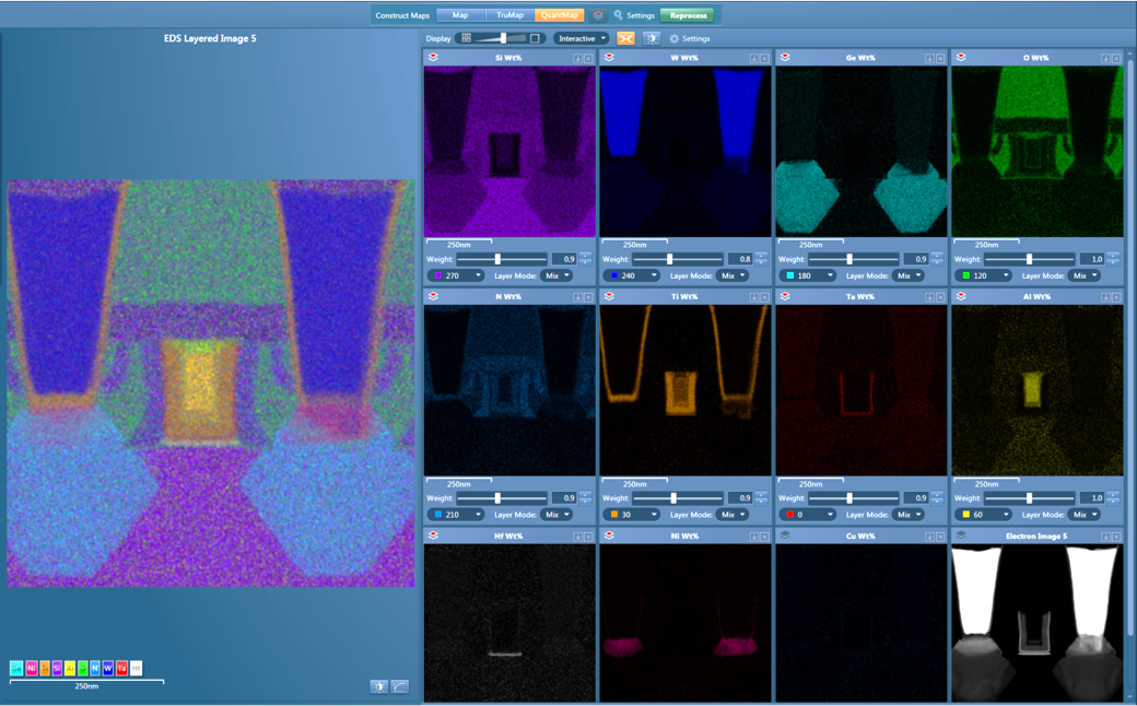
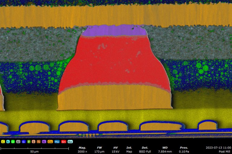
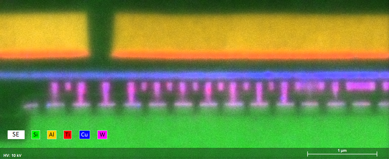
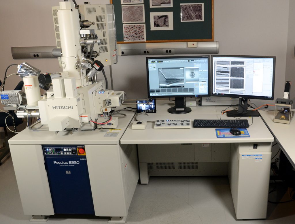
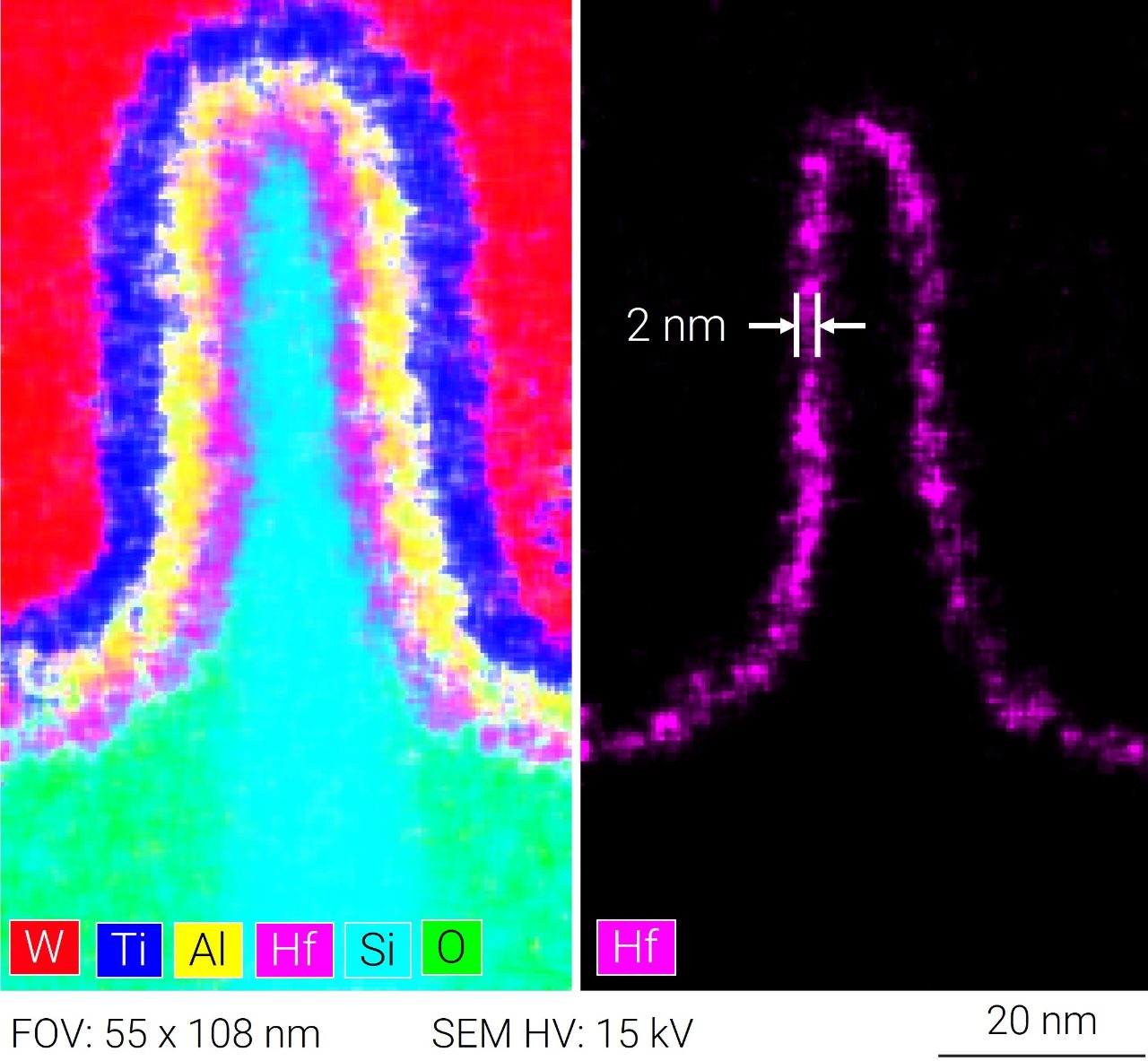
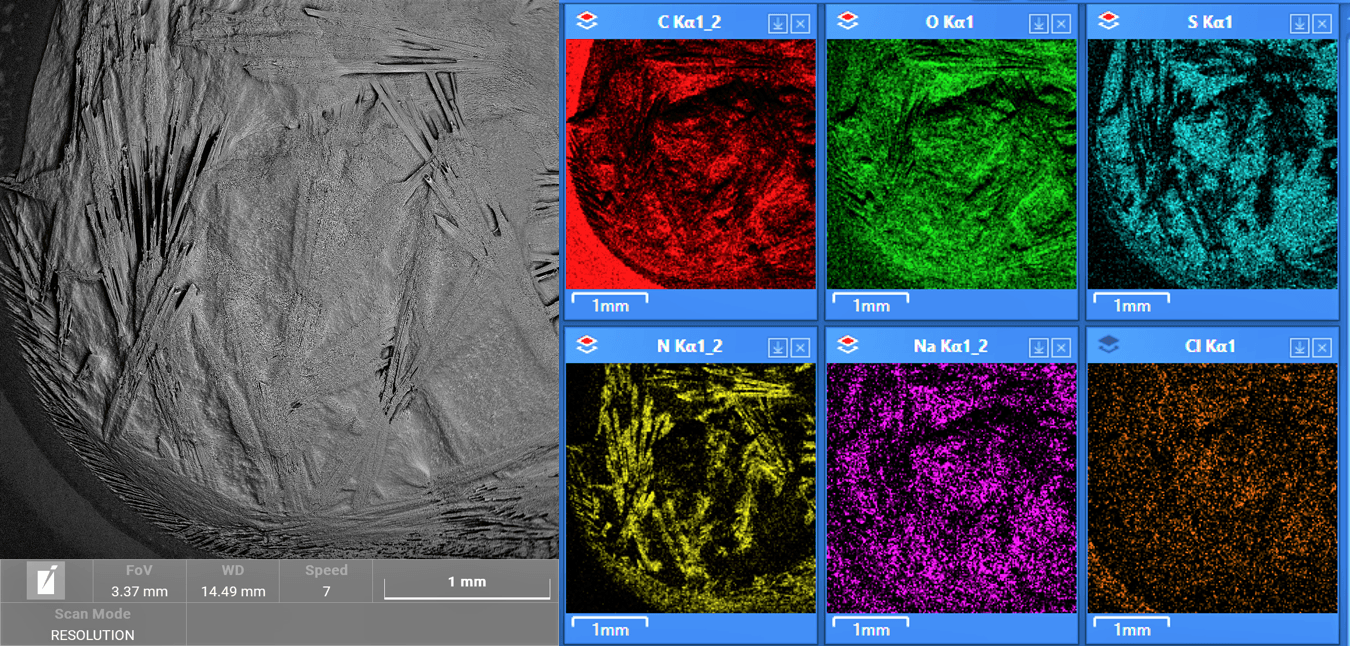
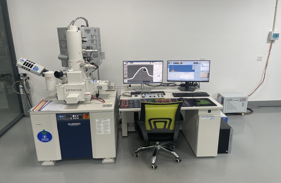
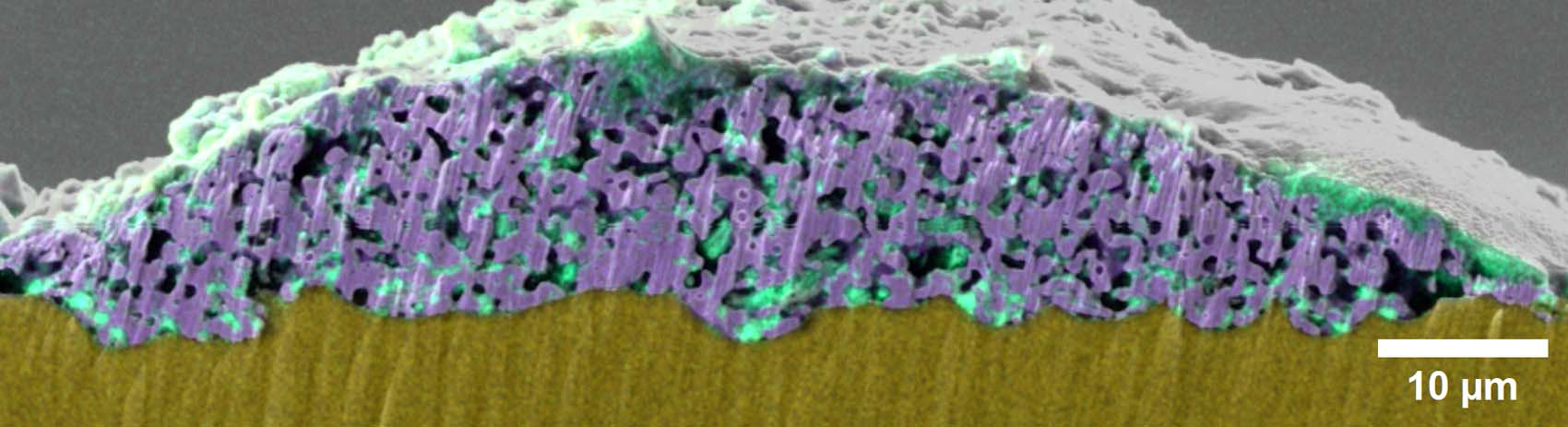
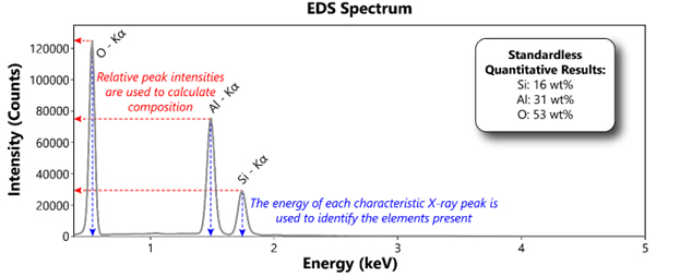
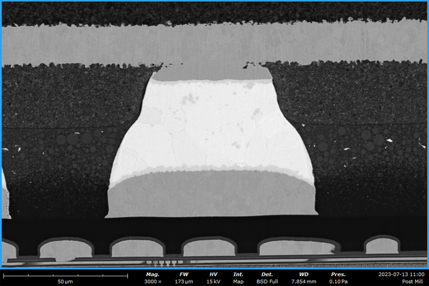
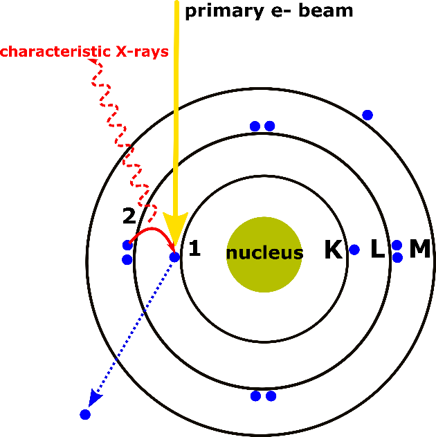
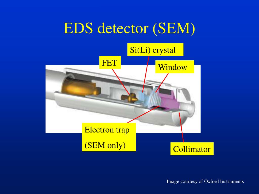
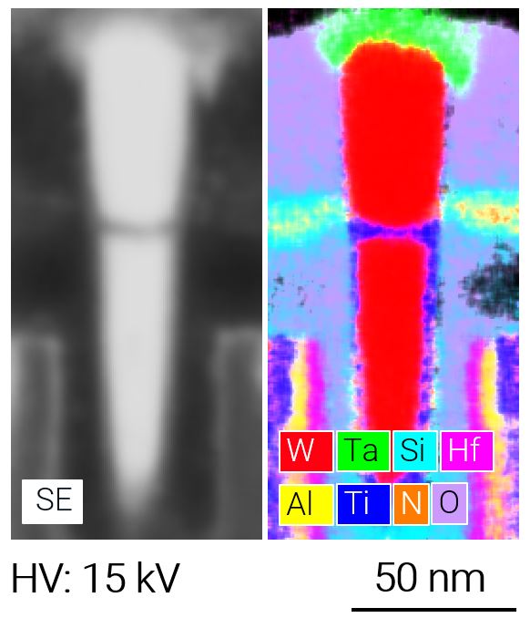
Sem/eds Semiconductor


.png?ver=53MTO8xuNRt8NTk2Zoan1w%3d%3d)


![Diagram of SEM with EDS detector [58] | Download Scientific Diagram](https://www.researchgate.net/profile/Andrew-Hamilton-6/publication/267503013/figure/fig18/AS:353236511936521@1461229555703/Diagram-of-SEM-with-EDS-detector-58.png)


Study the mechanics of Sem/eds Semiconductor through hundreds of technical photographs. illustrating the mechanical aspects of photography, images, and pictures. ideal for engineering and scientific applications. Our Sem/eds Semiconductor collection features high-quality images with excellent detail and clarity. Suitable for various applications including web design, social media, personal projects, and digital content creation All Sem/eds Semiconductor images are available in high resolution with professional-grade quality, optimized for both digital and print applications, and include comprehensive metadata for easy organization and usage. Discover the perfect Sem/eds Semiconductor images to enhance your visual communication needs. Cost-effective licensing makes professional Sem/eds Semiconductor photography accessible to all budgets. Each image in our Sem/eds Semiconductor gallery undergoes rigorous quality assessment before inclusion. The Sem/eds Semiconductor archive serves professionals, educators, and creatives across diverse industries. Reliable customer support ensures smooth experience throughout the Sem/eds Semiconductor selection process. Regular updates keep the Sem/eds Semiconductor collection current with contemporary trends and styles. Whether for commercial projects or personal use, our Sem/eds Semiconductor collection delivers consistent excellence. Professional licensing options accommodate both commercial and educational usage requirements. Time-saving browsing features help users locate ideal Sem/eds Semiconductor images quickly.