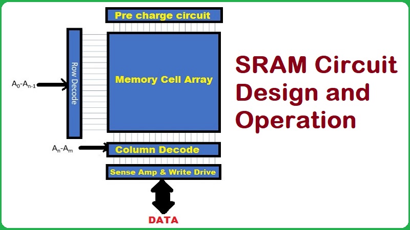
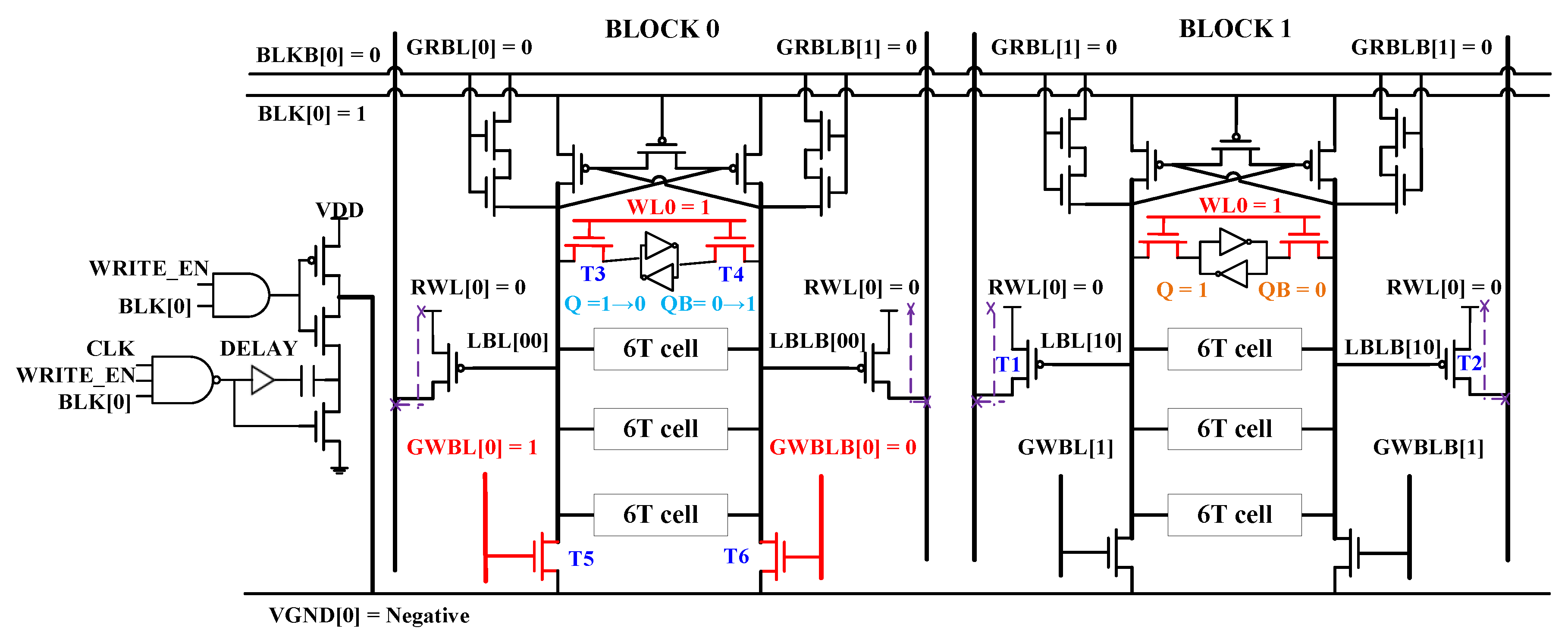
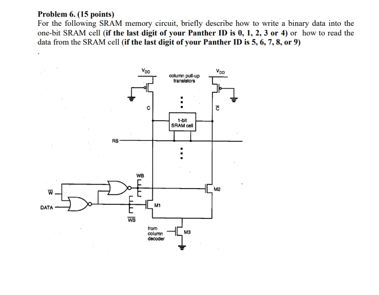
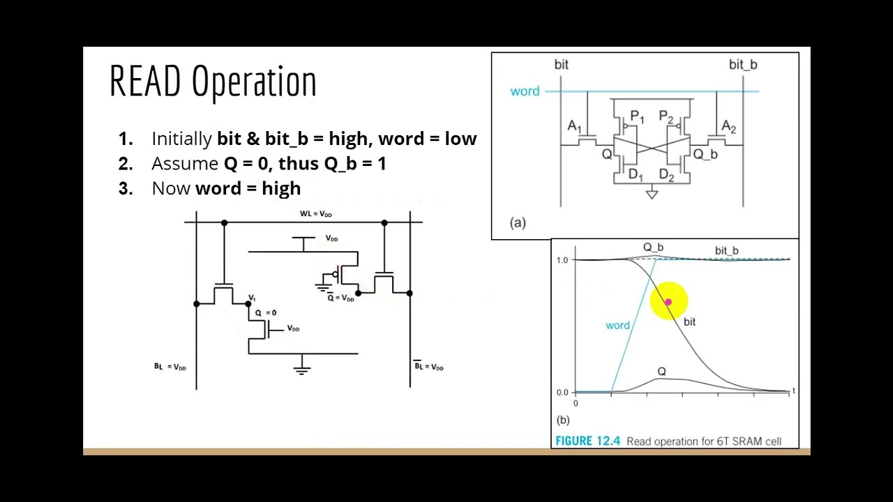
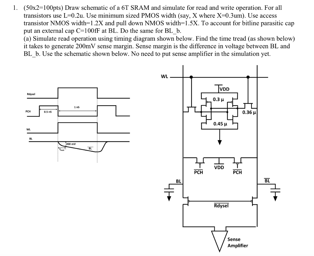
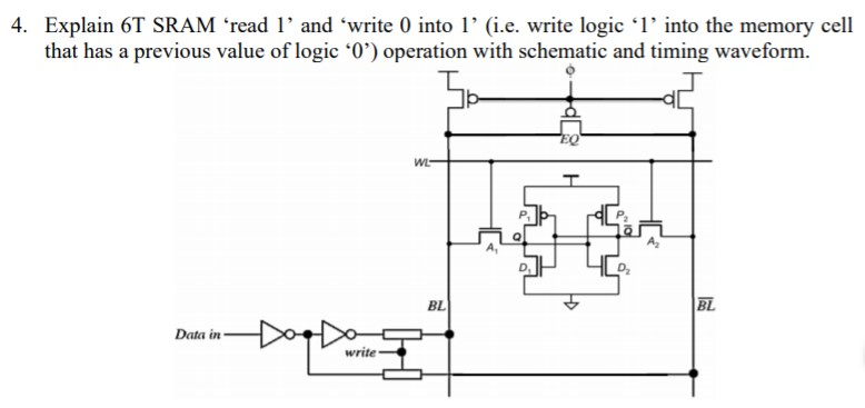
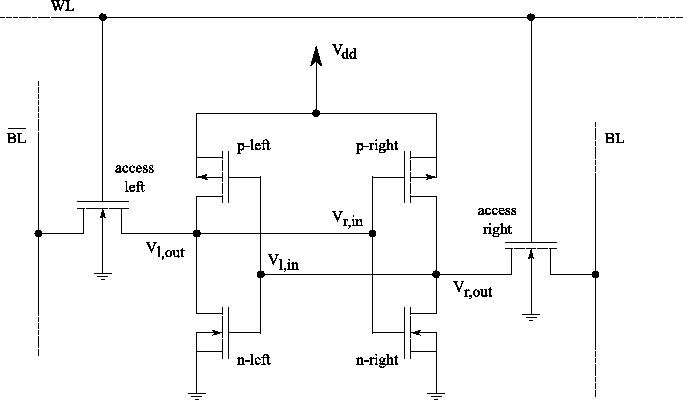
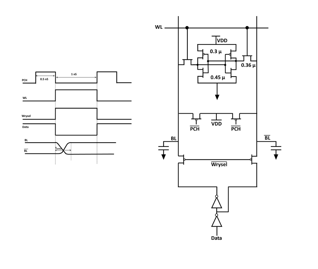
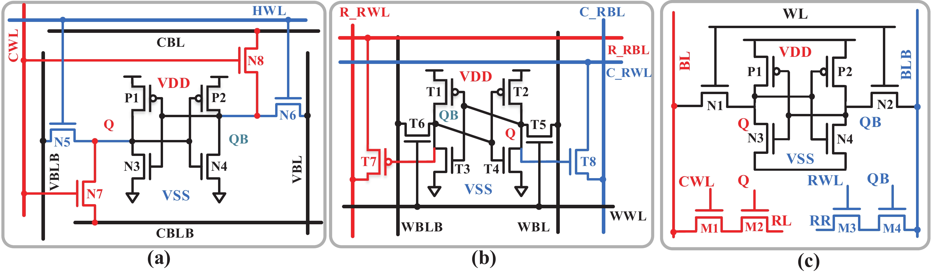
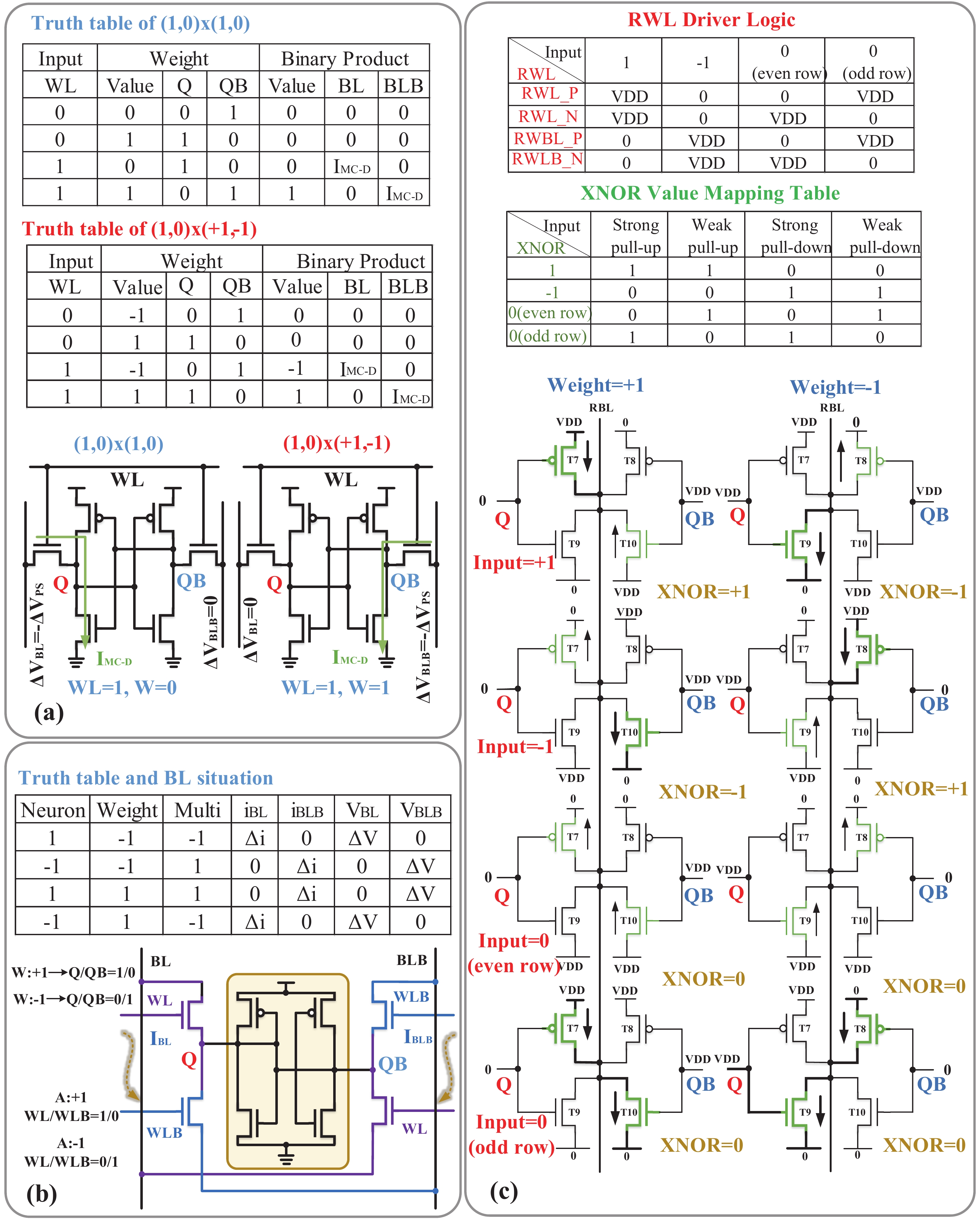
Read/write Circuit For Sram


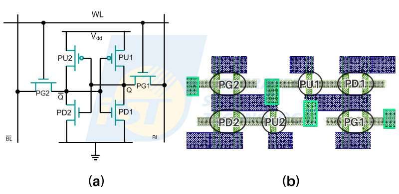
![shows the basic 6T SRAM cell circuit diagram [17]. PU1 and PU2 are the ...](https://www.researchgate.net/publication/339278293/figure/download/fig2/AS:858655498964992@1581730832272/shows-the-basic-6T-SRAM-cell-circuit-diagram-17-PU1-and-PU2-are-the-pull-up.png)


![Schematic of read and write circuits of the SRAM cell [6] and the ...](https://www.researchgate.net/publication/269577949/figure/fig4/AS:1034855328542721@1623740145218/Schematic-of-read-and-write-circuits-of-the-SRAM-cell-6-and-the-additional-logic-for.png)

![Schematic of read and write circuits of the SRAM cell [6] and the ...](https://www.researchgate.net/profile/Govind-Prasad-6/publication/269577949/figure/fig3/AS:1034855328538626@1623740145202/Schematic-of-proposed-SRAM-cell_Q640.jpg)
![Schematic of read and write circuits of the SRAM cell [6] and the ...](https://www.researchgate.net/profile/Siba-Panda/publication/320038694/figure/fig1/AS:542966533103616@1506464717457/T-SRAM-cell_Q640.jpg)

![Schematic of read and write circuits of the SRAM cell [6] and the ...](https://www.researchgate.net/publication/348452221/figure/fig1/AS:979896167849984@1610636860274/SRAM-Cell-22-Adiabatic-SRAM-The-8T-SRAM-cell-5-used-here-has-an-adiabatically_Q640.jpg)


![Schematic of read and write circuits of the SRAM cell [6] and the ...](https://www.researchgate.net/profile/Govind-Prasad-6/publication/269577949/figure/fig2/AS:1034855328530432@1623740145184/Schematic-of-NC-SRAM-Cell_Q320.jpg)

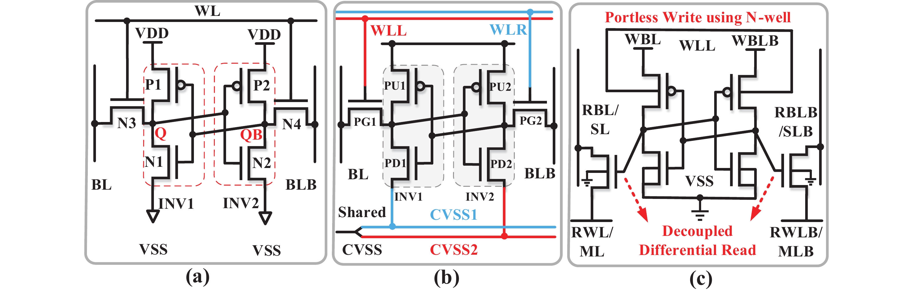
![Schematic of read and write circuits of the SRAM cell [6] and the ...](https://www.researchgate.net/profile/Govind-Prasad-6/publication/269577949/figure/fig1/AS:1034855328542720@1623740145163/Schematics-of-conventional-6T-SRAM-cell_Q320.jpg)


![Write '0' 0peration of 6T SRAM cell [1] [5] | Download Scientific Diagram](https://www.researchgate.net/publication/352619585/figure/fig3/AS:1037772747976705@1624435712927/Write-0-0peration-of-6T-SRAM-cell-1-5.jpg)


![Schematic of read and write circuits of the SRAM cell [6] and the ...](https://www.researchgate.net/publication/339267258/figure/fig3/AS:1093437524844555@1637707229378/Shorted-gate-SG-fin-type-field-effect-transistor-FinFET-static-random-access-memory_Q640.jpg)


![Schematic of read and write circuits of the SRAM cell [6] and the ...](https://www.researchgate.net/publication/348452221/figure/fig5/AS:979896167845889@1610636860641/b-MCPL-based-SRAM-Cell-with-Read-and-Write-Operation_Q320.jpg)


![[GET ANSWER] VDD BL BL WL PU1 PU2 N2 PG2 PG1 N1 PD1 PD2 GND Consider ...](https://cdn.numerade.com/ask_images/56d17a030e2a46bc8224e73c2b518511.jpg)

Dive into the stunning world of abstract Read/write Circuit For Sram with countless imaginative images. highlighting the innovative use of photography, images, and pictures. designed to inspire imagination and creativity. Discover high-resolution Read/write Circuit For Sram images optimized for various applications. Suitable for various applications including web design, social media, personal projects, and digital content creation All Read/write Circuit For Sram images are available in high resolution with professional-grade quality, optimized for both digital and print applications, and include comprehensive metadata for easy organization and usage. Explore the versatility of our Read/write Circuit For Sram collection for various creative and professional projects. Whether for commercial projects or personal use, our Read/write Circuit For Sram collection delivers consistent excellence. The Read/write Circuit For Sram archive serves professionals, educators, and creatives across diverse industries. Comprehensive tagging systems facilitate quick discovery of relevant Read/write Circuit For Sram content. The Read/write Circuit For Sram collection represents years of careful curation and professional standards. Multiple resolution options ensure optimal performance across different platforms and applications. Instant download capabilities enable immediate access to chosen Read/write Circuit For Sram images. Advanced search capabilities make finding the perfect Read/write Circuit For Sram image effortless and efficient.