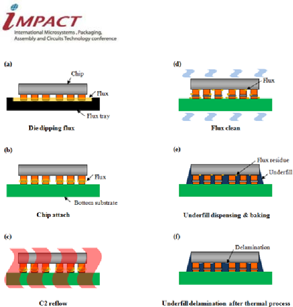
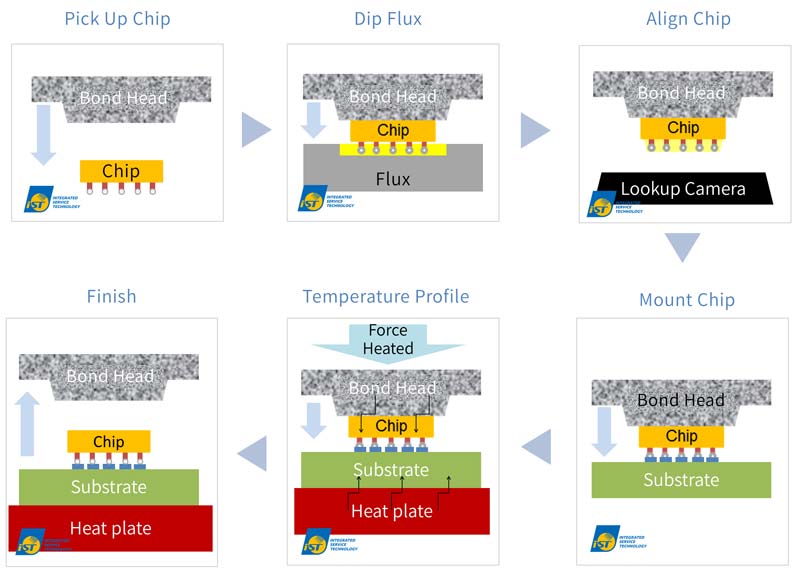
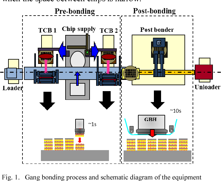
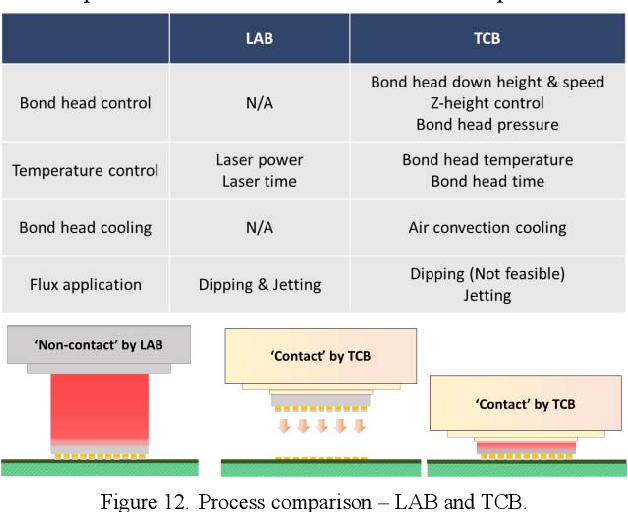
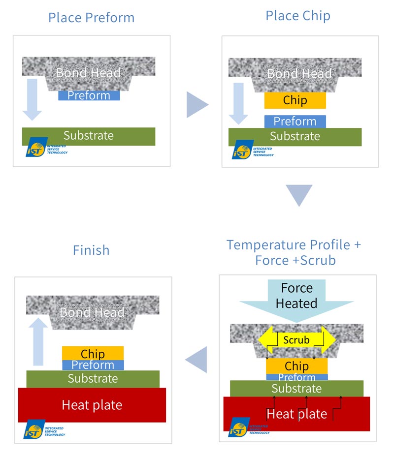
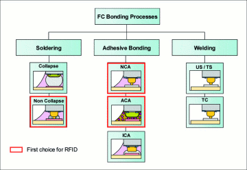
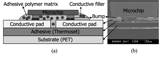
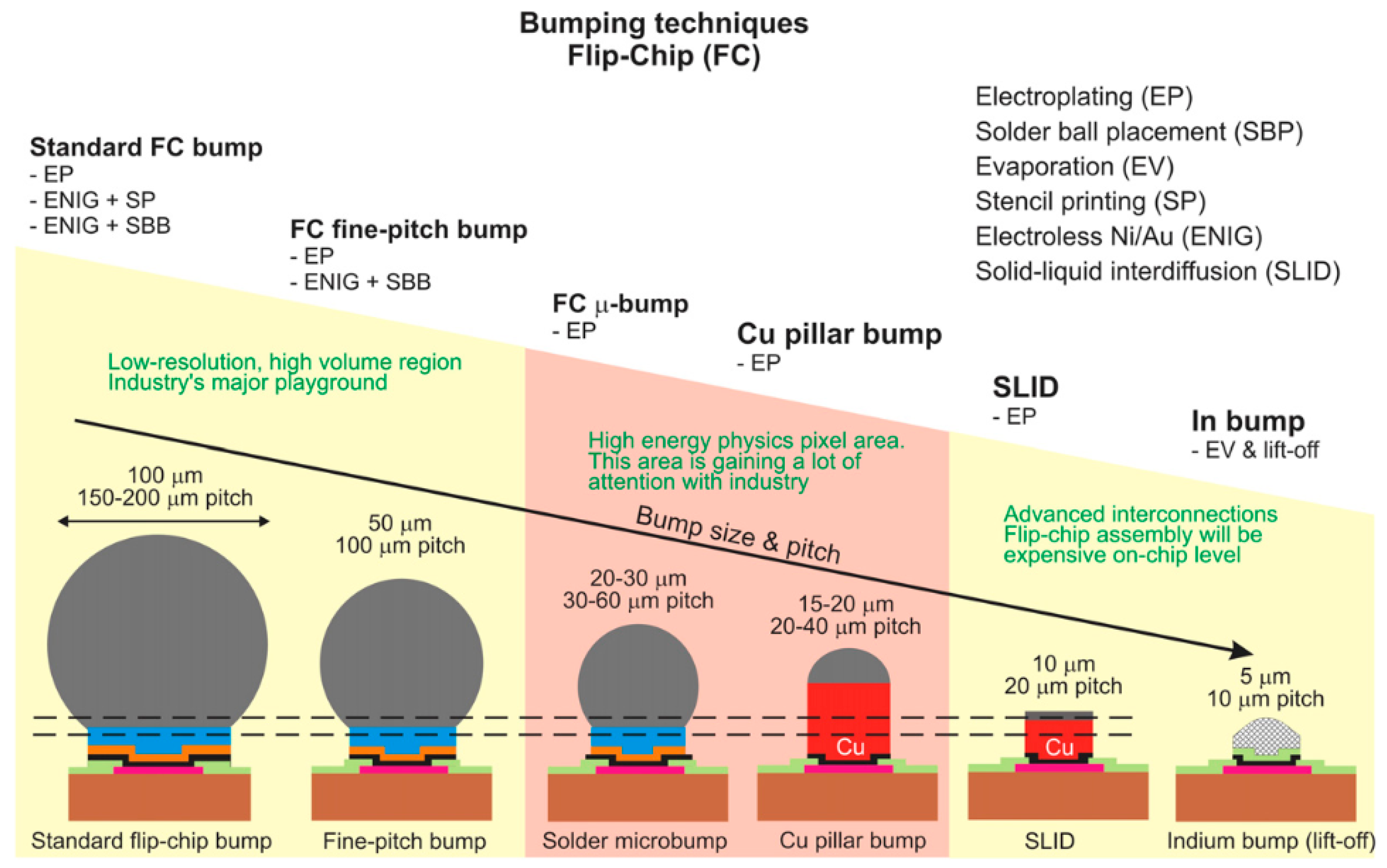
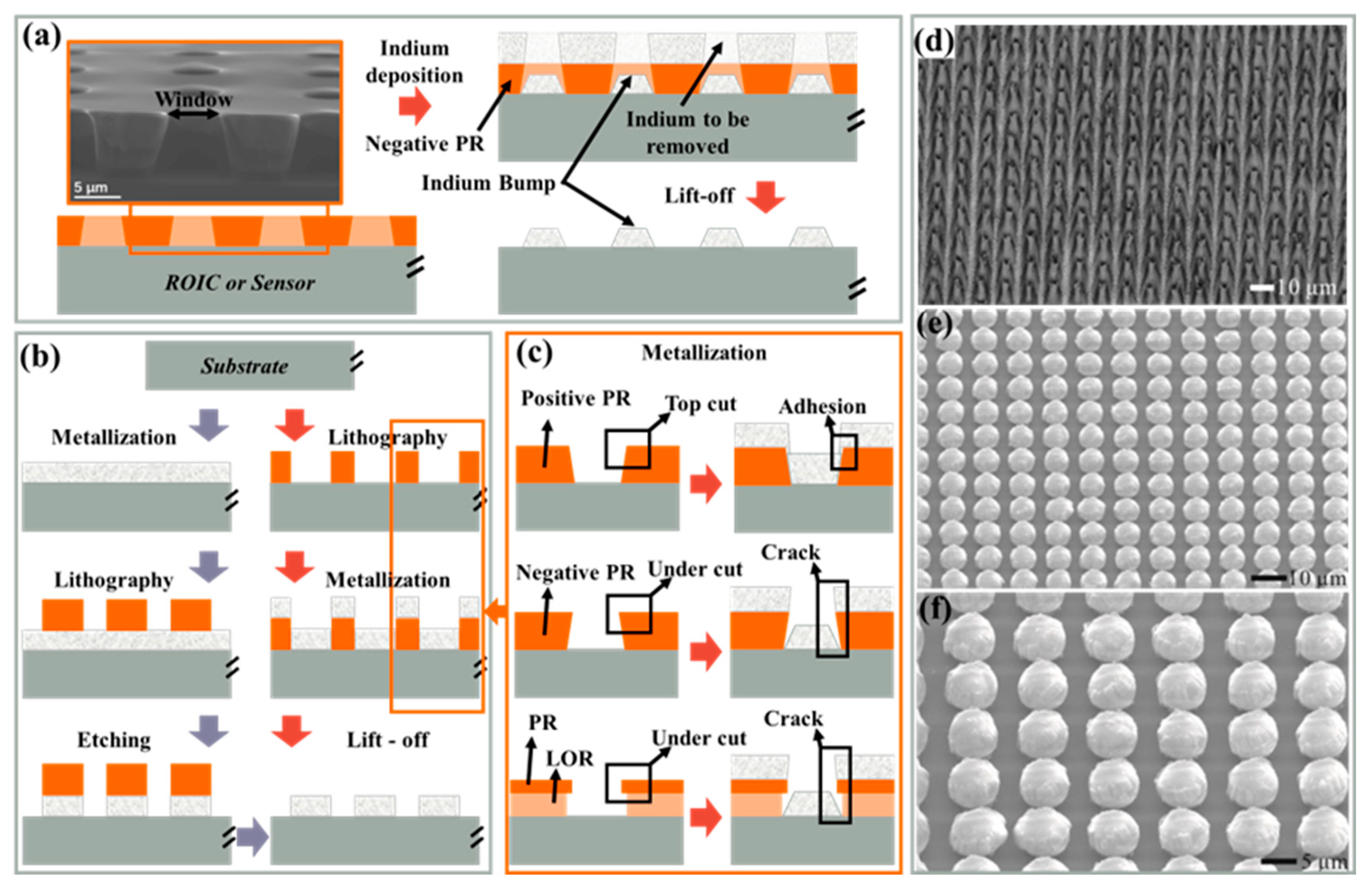
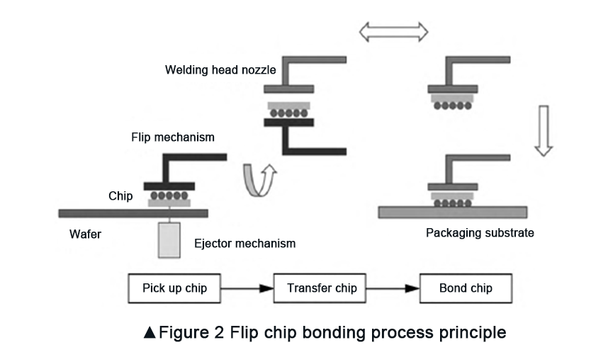
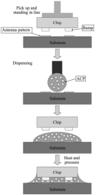
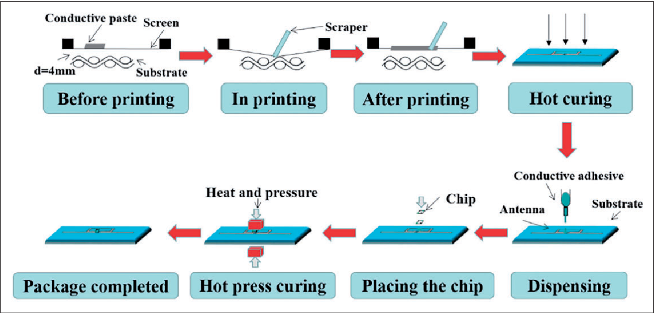
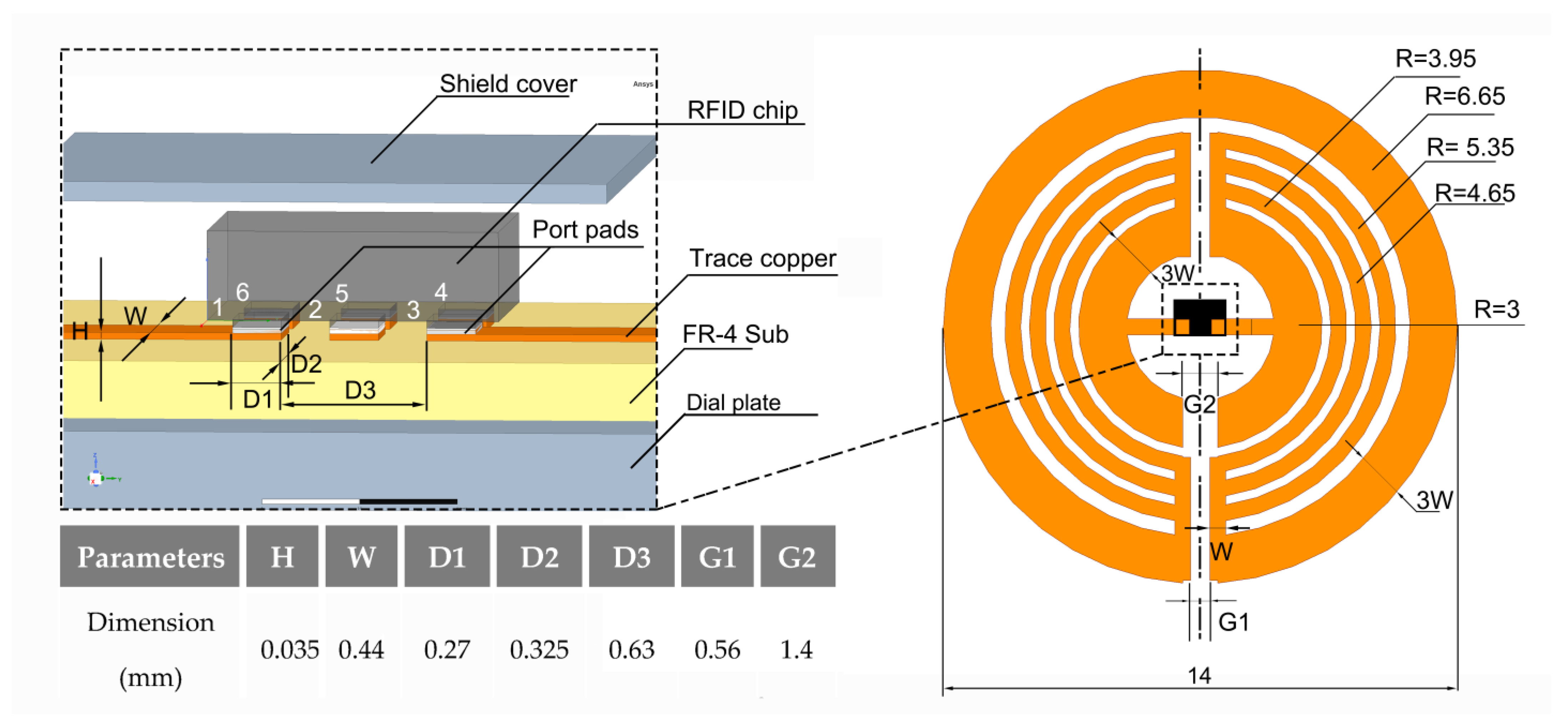
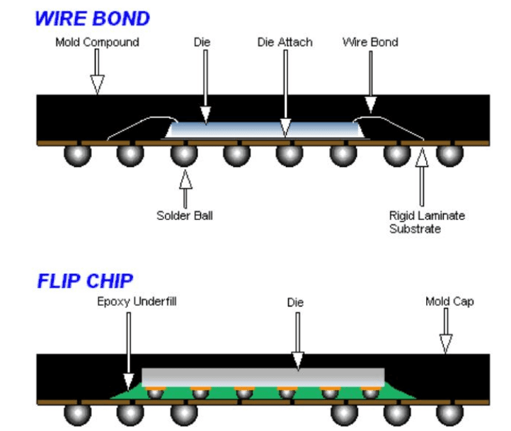
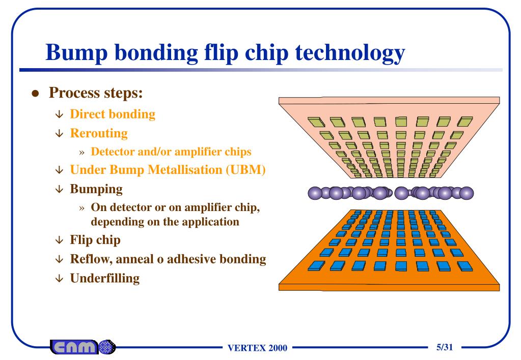
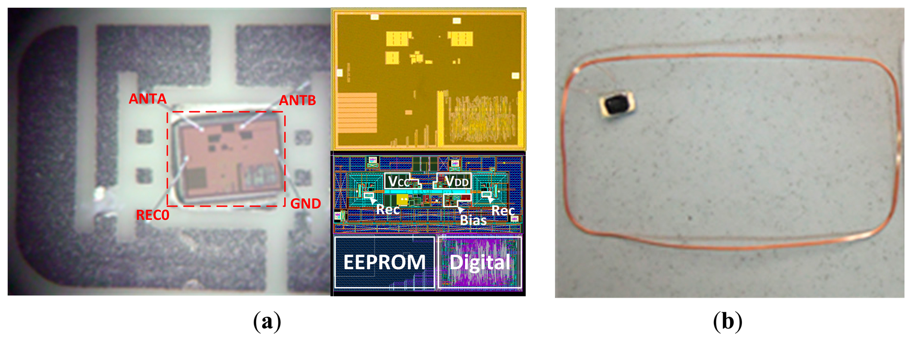
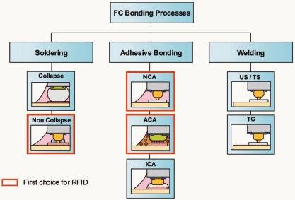
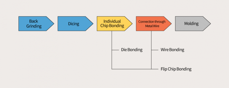
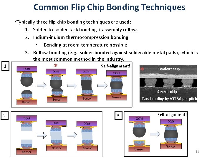
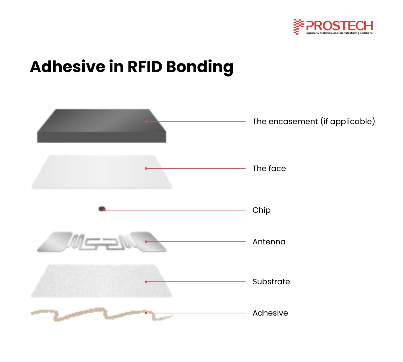
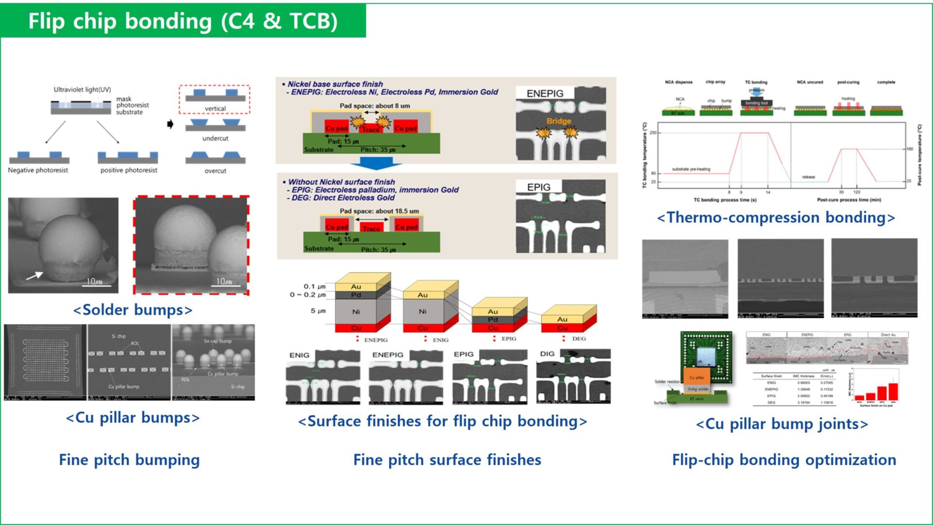
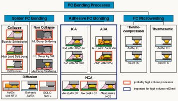
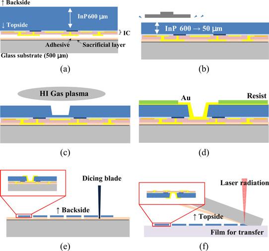
Rfid Chip Bonding Process Map


![RFID Working Process [12]. | Download Scientific Diagram](https://www.researchgate.net/profile/Muhammad-Ayoub-Kamal/publication/341787374/figure/fig1/AS:897509723500547@1590994401628/Fig-1-RFID-Working-Process-12.png)


Experience the stunning modern approach to Rfid Chip Bonding Process Map with vast arrays of contemporary images. featuring the latest innovations in photography, images, and pictures. designed to showcase innovation and progress. The Rfid Chip Bonding Process Map collection maintains consistent quality standards across all images. Suitable for various applications including web design, social media, personal projects, and digital content creation All Rfid Chip Bonding Process Map images are available in high resolution with professional-grade quality, optimized for both digital and print applications, and include comprehensive metadata for easy organization and usage. Our Rfid Chip Bonding Process Map gallery offers diverse visual resources to bring your ideas to life. Diverse style options within the Rfid Chip Bonding Process Map collection suit various aesthetic preferences. The Rfid Chip Bonding Process Map collection represents years of careful curation and professional standards. Professional licensing options accommodate both commercial and educational usage requirements. Regular updates keep the Rfid Chip Bonding Process Map collection current with contemporary trends and styles. Multiple resolution options ensure optimal performance across different platforms and applications. The Rfid Chip Bonding Process Map archive serves professionals, educators, and creatives across diverse industries. Time-saving browsing features help users locate ideal Rfid Chip Bonding Process Map images quickly.